- 您現在的位置:買賣IC網 > PDF目錄9028 > CY28346ZXCT (Silicon Laboratories Inc)IC CLOCK DIFF OUT CK408 56TSSOP PDF資料下載
參數資料
| 型號: | CY28346ZXCT |
| 廠商: | Silicon Laboratories Inc |
| 文件頁數: | 7/19頁 |
| 文件大小: | 0K |
| 描述: | IC CLOCK DIFF OUT CK408 56TSSOP |
| 標準包裝: | 2,000 |
| 類型: | * |
| PLL: | 是 |
| 輸入: | 晶體 |
| 輸出: | 時鐘 |
| 電路數: | 1 |
| 比率 - 輸入:輸出: | 1:19 |
| 差分 - 輸入:輸出: | 無/是 |
| 頻率 - 最大: | 200MHz |
| 除法器/乘法器: | 是/無 |
| 電源電壓: | 3.135 V ~ 3.465 V |
| 工作溫度: | 0°C ~ 70°C |
| 安裝類型: | * |
| 封裝/外殼: | * |
| 供應商設備封裝: | * |
| 包裝: | * |
| 其它名稱: | SLCY28346ZXCT |
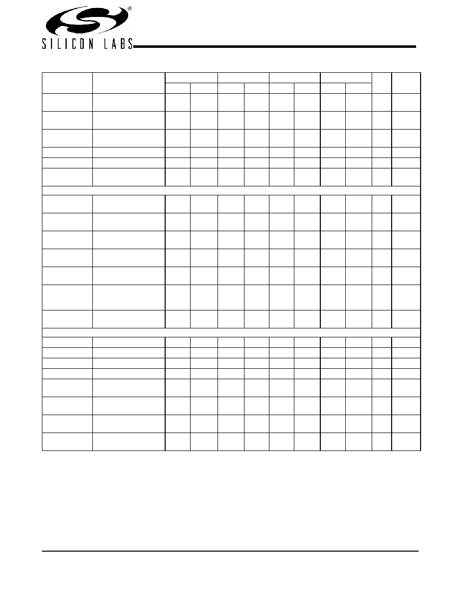
CY28346
......................Document #: 38-07331 Rev. *C Page 15 of 19
TCCJ
CPU Cycle to Cycle
Jitter
150
ps
TR/TF
CPUT and CPUC Rise
and Fall Times
175
700
175
700
175
700
175
700
ps
Rise/Fall Matching
20%
DeltaTR
Rise Time Variation
125
ps
DeltaTF
Fall Time Variation
125
ps
VCROSS
Crossing Point Voltage
at 0.7V Swing
280
430
280
430
280
430
280
430
mV
CPU at 1.0V Timing
TDC
CPUT and CPUC Duty
Cycle
45
55
45
55
45
55
45
55
%
TPERIOD
CPUT and CPUC
Period
14.85
15.3
9.85
10.2
7.35
7.65
4.85
5.1
nS
TSKEW
Any CPU to Any CPU
Clock Skew
100
pS
TCCJ
CPU Cycle to Cycle
Jitter
150
pS
Differential
TR/TF
CPUT and CPUC Rise
and Fall Times
175
467
175
467
175
467
175
467
ps
SE–
DeltaSlew
Absolute Single- ended
Rise/Fall Waveform
Symmetry
325
ps
VCROSS
Cross Point at 1.0V
swing
510
760
510
760
510
760
510
760
mV
3V66
TDC
3V66 Duty Cycle
45
55
45
55
45
55
45
55
%
TPERIOD
3V66 Period
15.0
15.3
15.0
15.3
15.0
15.3
15.0
15.3
ns
THIGH
3V66 HIGH Time
4.95
ns
TLOW
3V66 LOW Time
4.55
ns
TR/TF
3V66 Rise and Fall
Times
0.5
2.0
0.5
2.0
0.5
2.0
0.5
2.0
ns
TSKEW
Unbuffered
3V66 to 3V66 Clock
Skew
500
ps
TSKEW
Buffered
3V66 to 3V66 Clock
Skew
250
ps
TCCJ
DRCG Cycle to Cycle
Jitter
250
ps
Notes:
20. Measurement taken from differential waveform, from –0.35V to +0.35V.
21. Measurements taken from common mode waveforms, measure rise/fall time from 0.41 to 0.86V. Rise/fall time matching is defined as “the instantaneous difference
between maximum CLK rise (fall) and minimum CLK# fall (rise) time or minimum CLK rise (fall) and maximum CLK# fall (rise) time.” This parameter is designed
form waveform symmetry.
22. Measured in absolute voltage, i.e., single-ended measurement.
23. THIGH is measured at 2.4V for non-host outputs.
24. TLOW is measured at 0.4V for all outputs.
25. Probes are placed on the pins, and measurements are acquired between 0.4V and 2.4V for 3.3V signals (see test and measurement set-up section of this data
sheet).
AC Parameters (VDD = VDDA = 3.3V ±5%, TA = 0°C to +70°C) (continued)
Parameter
Description
66 MHz
100 MHz
133 MHz
200 MHz
Unit
Notes
Min.
Max.
Min.
Max.
Min.
Max.
Min.
Max.
相關PDF資料 |
PDF描述 |
|---|---|
| CY28346ZXC-2T | IC CLOCK DIFF OUT CK408 56TSSOP |
| CY28346OXCT | IC CLOCK DIFF OUT CK408 56SSOP |
| MPC9653AACR2/W | IC PLL CLK GEN 1:8 3.3V 32-LQFP |
| MPC9653AACR2 | IC PLL CLK GEN 1:8 3.3V 32-LQFP |
| VE-J72-MZ-F3 | CONVERTER MOD DC/DC 15V 25W |
相關代理商/技術參數 |
參數描述 |
|---|---|
| CY28347 | 制造商:CYPRESS 制造商全稱:Cypress Semiconductor 功能描述:Universal Single-chip Clock Solution for VIA P4M266/KM266 DDR Systems |
| CY28347OC | 制造商:CYPRESS 制造商全稱:Cypress Semiconductor 功能描述:Universal Single-chip Clock Solution for VIA P4M266/KM266 DDR Systems |
| CY28347OCT | 制造商:CYPRESS 制造商全稱:Cypress Semiconductor 功能描述:Universal Single-chip Clock Solution for VIA P4M266/KM266 DDR Systems |
| CY28347ZC | 制造商:Rochester Electronics LLC 功能描述:- Bulk |
| CY28347ZCT | 制造商:Rochester Electronics LLC 功能描述:FTG FOR VIA P4 CHIPSET - Tape and Reel |
發(fā)布緊急采購,3分鐘左右您將得到回復。