- 您現(xiàn)在的位置:買賣IC網(wǎng) > PDF目錄374147 > CGY2010G (NXP SEMICONDUCTORS) GSM 4 W power amplifiers PDF資料下載
參數(shù)資料
| 型號: | CGY2010G |
| 廠商: | NXP SEMICONDUCTORS |
| 元件分類: | 衰減器 |
| 英文描述: | GSM 4 W power amplifiers |
| 中文描述: | 880 MHz - 915 MHz RF/MICROWAVE NARROW BAND HIGH POWER AMPLIFIER |
| 文件頁數(shù): | 5/12頁 |
| 文件大小: | 79K |
| 代理商: | CGY2010G |
1996 Jul 08
5
Philips Semiconductors
Objective specification
GSM 4 W power amplifiers
CGY2010G; CGY2011G
FUNCTIONAL DESCRIPTION
Operating conditions
The CGY2010G and CGY2011G are designed to meet the
European Telecommunications Standards Institute (ETSI)
GSM documents, the “ETS 300 577 specification” which
are defined as follows:
t
on
= 542.8
μ
s
T = 4.3 ms
Duty cycle = 1/8
The devices are specifically designed for pulse operation
allowing the use of a LQFP48 plastic package.
Power amplifier
The power amplifier consists of four cascaded gain stages
with an open-drain configuration. Each drain has to be
loaded externally by an adequate reactive circuit which
also has to be a DC path to the supply.
The amplifier bias is set by means of a negative voltage
applied at pins V
GG1
and V
GG2
. This negative voltage must
be present before the supply voltage is applied to the
drains to avoid current overstress for the amplifier.
Power sensor driver
The power sensor driver is a buffer amplifier that delivers
a signal to the DETO output pin which is proportional to the
amplifier power. This signal can be detected by external
diodes for power control purpose. As the sensor signal is
taken from the input of the last stage of the PA, it is isolated
from disturbances at the output by the reverse isolation of
the PA output stage.
Impedance mismatch at the PA output therefore, does not
significantly influence the signal delivered by the power
sensor as this normally occurs when power sense is made
using a directional coupler. Consequently the cost and
space of using a directional coupler are saved.
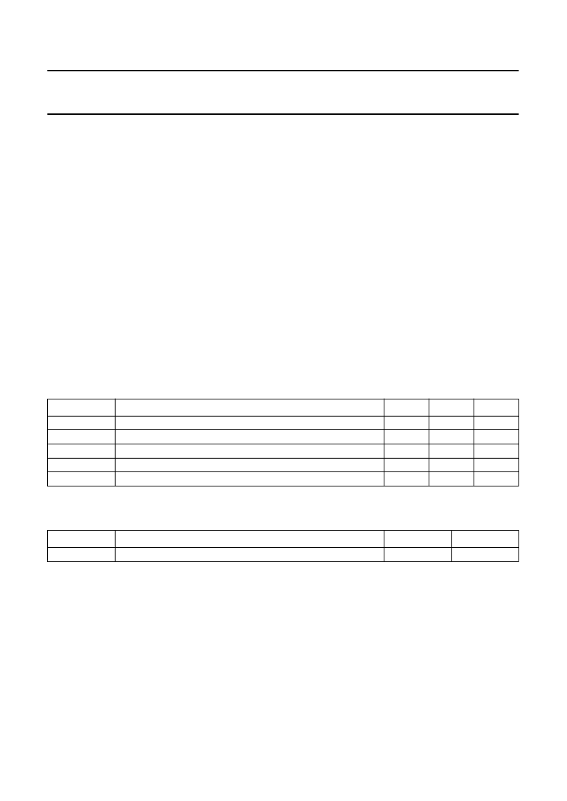
LIMITING VALUES
In accordance with the Absolute Maximum Rating System (IEC 134); general operating conditions applied.
THERMAL CHARACTERISTICS
General operating conditions applied.
Note
1.
This thermal resistance is measured under GSM pulse conditions.
SYMBOL
PARAMETER
MIN.
MAX.
UNIT
V
DD
V
GG
T
j(max)
T
stg
P
tot
positive supply voltage
negative supply voltage
maximum operating junction temperature
IC storage temperature
total power dissipation
7
10
150
150
1.5
V
V
°
C
°
C
W
SYMBOL
PARAMETER
VALUE
UNIT
R
th j-c
thermal resistance from junction to case; note 1
32
K/W
相關(guān)PDF資料 |
PDF描述 |
|---|---|
| CGY2011G | GSM 4 W power amplifiers |
| CGY2013G | GSM 4 W power amplifier |
| CGY2014 | GSM/DCS/PCS power amplifier |
| CGY2014ATW | GSM/DCS/PCS power amplifier |
| CGY2021G | DCS/PCS 2 W power amplifier |
相關(guān)代理商/技術(shù)參數(shù) |
參數(shù)描述 |
|---|---|
| CGY2011G | 制造商:PHILIPS 制造商全稱:NXP Semiconductors 功能描述:GSM 4 W power amplifiers |
| CGY2013G | 制造商:PHILIPS 制造商全稱:NXP Semiconductors 功能描述:GSM 4 W power amplifier |
| CGY2014 | 制造商:PHILIPS 制造商全稱:NXP Semiconductors 功能描述:GSM/DCS/PCS power amplifier |
| CGY2014ATW | 制造商:PHILIPS 制造商全稱:NXP Semiconductors 功能描述:GSM/DCS/PCS power amplifier |
| CGY2014TT | 制造商:未知廠家 制造商全稱:未知廠家 功能描述:MICROWAVE/MILLIMETER WAVE AMPLIFIER|DUAL|GAAS|TSSOP|20PIN|PLASTIC |
發(fā)布緊急采購,3分鐘左右您將得到回復(fù)。