- 您現(xiàn)在的位置:買賣IC網(wǎng) > PDF目錄379831 > CDC9163 (Texas Instruments, Inc.) PC Motherboard Clock Sythesizer/Drivers with SDRAM Clock Support(PC時(shí)鐘合成器/驅(qū)動(dòng)器(SDRAM 時(shí)鐘支持)) PDF資料下載
參數(shù)資料
| 型號(hào): | CDC9163 |
| 廠商: | Texas Instruments, Inc. |
| 英文描述: | PC Motherboard Clock Sythesizer/Drivers with SDRAM Clock Support(PC時(shí)鐘合成器/驅(qū)動(dòng)器(SDRAM 時(shí)鐘支持)) |
| 中文描述: | 電腦主板時(shí)鐘Sythesizer /支持與SDRAM時(shí)鐘驅(qū)動(dòng)器(電腦時(shí)鐘合成器/驅(qū)動(dòng)器(SDRAM的時(shí)鐘支持)) |
| 文件頁(yè)數(shù): | 1/9頁(yè) |
| 文件大小: | 177K |
| 代理商: | CDC9163 |
CDC9163
PC CLOCK SYNTHESIZER/DRIVER
WITH SDRAM CLOCK SUPPORT
SCAS574 – JULY 1996
1
POST OFFICE BOX 655303
DALLAS, TEXAS 75265
Clock Generation for Pentium
/430VX
Motherboards
Twelve Host Clock Outputs With
Programmable Frequency
Six PCI Clock Outputs
One Serial Bus 48-MHz Clock
One Floppy Controller 24-MHz Clock
Two Reference 14.318-MHz Clock Outputs
All Output Clock Frequencies Derived From
a Single 14.31818-MHz Crystal Input
Internal Loop Filters for Phase-Lock Loops
(PLLs)
Power-Down Modes
Packaged in Plastic Shrink Small-Outline
Package
description
The CDC9163 is an integrated clock synthesizer
specifically designed for use in Pentium
/430VX
based motherboards. Twelve host clock outputs
(HCLKn) are programmable via the SEL(0:2)
control inputs. This allows four HCLK clocks for
use with the processor and chipset, and eight
HCLK clocks for use with synchronous DRAM
dual in-line memory modules (SDRAM DIMM).
The CDC9163 provides six copies of the PCI clock
(PCIn), which can be disabled via the PCI_EN
control input. All PCI clocks operate at one-half the host clock frequency, and are offset 1 ns to 4 ns from the
rising edge of the host clock. In addition, the CDC9163 generates a 48-MHz serial bus clock (SBCLK), a 24-MHz
floppy controller clock, and two copies of the 14.318-MHz reference clock (REFn). All output frequencies are
generated from a 14.31818-MHz crystal or oscillator input.
PLLs are used to generate the host clock and serial bus clock frequencies. On-chip loop filters and internal
feedback eliminate the need for external components. The PCI clock frequency is derived from the base host
clock frequency, while the floppy controller clock is derived from the serial bus clock frequency.
The host and PCI clock outputs provide low-skew/low-jitter clock signals for reliable clock operation. All outputs
are 3 state and are disabled via the output-enable (OE) input. When OE is high, all outputs are enabled. When
OE is low, the outputs are disabled to a high-impedance state. An internal pullup resistor is provided on OE.
Low-power operation also is provided for with HCLK_EN and PCI_EN inputs. HCLK_EN, when low, places all
host clocks in the logic low state; all other outputs operate normally. PCI_EN, when low, places all PCI clocks
in the logic low state; all other outputs operate normally. Internal pulldown resistors are provided on the
HCLK_EN and PCI_EN inputs.
Because the CDC9163 is based on PLL circuitry, it requires a stabilization time to achieve phase-lock of the PLL.
This stabilization time is required following power-up and application of a fixed-frequency, fixed-phase signal
at the XIN input, as well as following any changes to SEL(0:2).
Copyright
1996, Texas Instruments Incorporated
PRODUCT PREVIEW information concerns products in the formative or
design phase of development. Characteristic data and other
specifications are design goals. Texas Instruments reserves the right to
change or discontinue these products without notice.
Please be aware that an important notice concerning availability, standard warranty, and use in critical applications of
Texas Instruments semiconductor products and disclaimers thereto appears at the end of this data sheet.
Pentium is a trademark of Intel Corporation.
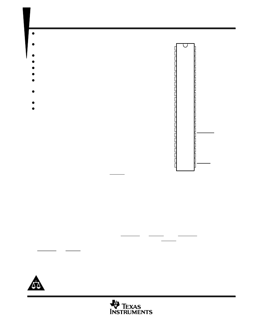
DL PACKAGE
(TOP VIEW)
1
2
3
4
5
6
7
8
9
10
11
12
13
14
15
16
17
18
19
20
21
22
23
24
48
47
46
45
44
43
42
41
40
39
38
37
36
35
34
33
32
31
30
29
28
27
26
25
REF1
REF0
GND
XIN
XOUT
V
CC(CPU)
SEL2
HCLK12
HCLK11
GND
PCI1
PCI2
PCI3
PCI4
V
CC(PCI)
PCI5
PCI6
GND
GND
V
CC
V
CC
FCCLK
SBCLK
GND
V
CC
HCLK1
V
CC(CPU)
HCLK2
GND
GND
HCLK3
HCLK4
V
CC(CPU)
HCLK5
HCLK6
HCLK7
HCLK8
GND
HCLK9
HCLK10
V
CC(CPU)
HCLK_EN
GND
OE
V
CC
SEL0
SEL1
PCI_EN
P
相關(guān)PDF資料 |
PDF描述 |
|---|---|
| CDC9171 | DVD System Clock Synthesizerers(DVD系統(tǒng)時(shí)鐘合成器) |
| CDC9441 | DVD System Clock Synthesizerers(PC時(shí)鐘合成器/驅(qū)動(dòng)器(SDRAM 時(shí)鐘支持)) |
| CDC9449 | PC Motherboard Clock Sythesizer/Drivers with SDRAM Clock Support(PC時(shí)鐘合成器/驅(qū)動(dòng)器(SDRAM 時(shí)鐘支持)) |
| CDC9841 | PC MOTHERBOARD CLOCK SYNTHESIZER/DRIVER WITH 3-STATE OUTPUTS |
| CDC9841DW | PC MOTHERBOARD CLOCK SYNTHESIZER/DRIVER WITH 3-STATE OUTPUTS |
相關(guān)代理商/技術(shù)參數(shù) |
參數(shù)描述 |
|---|---|
| CDC921 | 制造商:TI 制造商全稱:Texas Instruments 功能描述:DIRECT RAMBUSE CLOCK GENERATOR |
| CDC921DL | 制造商:Texas Instruments 功能描述: |
| CDC922 | 制造商:TI 制造商全稱:Texas Instruments 功能描述:DIRECT RAMBUSE CLOCK GENERATOR |
| CDC922DL | 制造商:TI 制造商全稱:Texas Instruments 功能描述:133-MHz CLOCK SYNTHESIZER/DRIVER FOR PC MOTHERBOARDS WITH 3-STATE OUTPUTS |
| CDC922DLR | 制造商:Rochester Electronics LLC 功能描述:- Bulk |
發(fā)布緊急采購(gòu),3分鐘左右您將得到回復(fù)。