- 您現(xiàn)在的位置:買賣IC網(wǎng) > PDF目錄379668 > AN10E40 (Electronic Theatre Controls, Inc.) Field Programmable Analog Array PDF資料下載
參數(shù)資料
| 型號: | AN10E40 |
| 廠商: | Electronic Theatre Controls, Inc. |
| 英文描述: | Field Programmable Analog Array |
| 中文描述: | 現(xiàn)場可編程模擬陣列 |
| 文件頁數(shù): | 26/36頁 |
| 文件大小: | 293K |
| 代理商: | AN10E40 |
第1頁第2頁第3頁第4頁第5頁第6頁第7頁第8頁第9頁第10頁第11頁第12頁第13頁第14頁第15頁第16頁第17頁第18頁第19頁第20頁第21頁第22頁第23頁第24頁第25頁當(dāng)前第26頁第27頁第28頁第29頁第30頁第31頁第32頁第33頁第34頁第35頁第36頁
22
BVDD and BVSS
BVDD and BVSS supply all the band-gap voltage references, VMR generator and bias current generators. Here
again, the typical connection is to AVDD and AVSS.
ESD_VDD and ESD_VSS
These two signals do not normally source or sink any current to the AN10E40. In the rare event that a device pin is
electrically overstressed by an ESD or EOS event (Electrostatic Discharge or Electrical Overstress), then current is
sourced or sunk though these rails. These two should be connected to quiet supplies and here again AVDD and
AVSS are the typical connections.
CFG_VDD and CFG_VSS
The CFG_VDD and CFG_VSS rails supply all the digital configuration circuitry, the on board ring oscillator, APOR
and POR generation circuitry with +5V and 0V respectively. With the possible exception of the on board ring
oscillator, any digital supply noise produced by this circuitry would not normally effect the performance of the
analog portion, so no particular care need be taken with these supply signals from the chip’s point of view. Your
system however may have both “noisy” and “clean” power rails available. If so, CFG_Vxx may be best connected
to the “noisy” rail, leaving the “clean” supply as unpolluted as possible.
OPAMVMR and CEXT
As mentioned above in the Voltage Mid-Rail Generator section, both OPAMPVMR and CEXT should be bypassed
to a quiet ground node to ensure optimal performance. Generally, a good configuration consists of a Polyester
(Mylar) 10nF capacitor between CEXT and AVSS. A similar bypassing connection for OPAMPVMR is also
recommended. Care should be exercised in the placement of these components to minimize the signal path
between the array and the bypass capacitors.
The AN10E40 in Split Supply Systems
Electrical Parameters
Because the AN10E40 is programmable, performance characteristics are reported for representative pieces of the
device rather than for the entire device. The following graphs and numbers provide you with conservative estimates
of the sort of performance you can expect for your particular design.
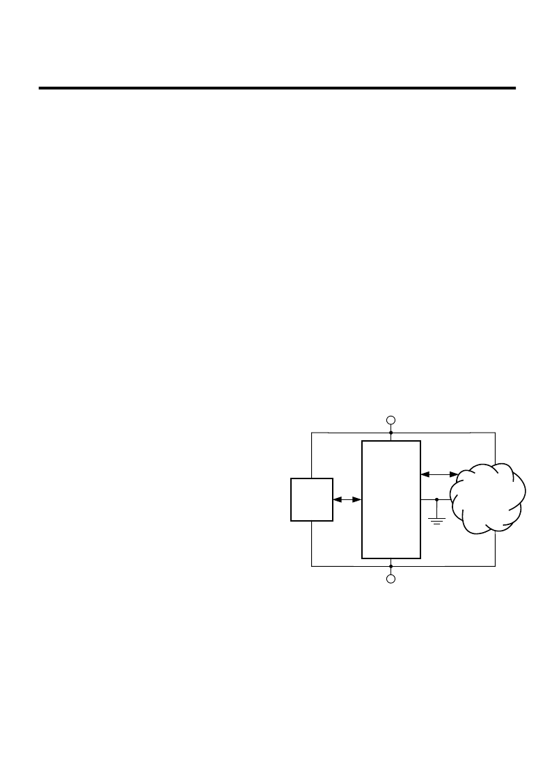
All analog signal processing within the AN10E40 is
referenced to its internal VMR node (Voltage Mid Rail,
normally 2.5 V above AVSS). For those applications
where a split supply (±2.5 V) is necessary, it is
possible to connect the AN10E40 as shown in Figure
20.
Here the AN10E40's internal VMR generator is
disabled (a feature available via AnadigmDesigner)
and the chip's VMR pin is instead driven externally by
the system's ground plane.
Naturally, logic circuits which interface to the AN10E40
must also be powered off the split rail as shown.
Under some circumstances, it may be more practical
to instead power the AN10E40 off a single 5 V supply
and AC coupled the ground referenced input signal.
AN10E40
Ground
Referenced
Analog
System
VDD
VMR
VSS
Boot
PROM
(or Micro)
+2.5 V
-2.5 V
Analog
Interface
Figure 20. Connecting to a Split Rail System
相關(guān)PDF資料 |
PDF描述 |
|---|---|
| AN17850A | Silicon Monolithic Bipolar IC |
| AN19 | AN19 - How 2 Use de KITS SPC DC Motor with StarTech PPI Card |
| AN2110S | JT 66C 66#22D SKT RECP |
| AN220D04-DEVLP | DANAMICALLY RECONFIGURABLE FPAA |
| AN220D04-EVAL | DANAMICALLY RECONFIGURABLE FPAA |
相關(guān)代理商/技術(shù)參數(shù) |
參數(shù)描述 |
|---|---|
| AN10-N01 | 制造商:SMC Corporation of America 功能描述:Silencer, Compact Resin, Male Thread, 1/8" NPT Port, 30 dB(A), Model AN10 |
| AN110 | 制造商:SILABS 制造商全稱:SILABS 功能描述:16-BIT PWM USING AN ON-CHIP TIMER |
| AN110-01 | 制造商:SMC Corporation of America 功能描述:MUFFLER 1/8 PT 制造商:SMC 功能描述:TCT Bulk |
| AN11006 | 制造商:PHILIPS 制造商全稱:NXP Semiconductors 功能描述:Single stage 2.3_2.7GHz LNA with BFU730F |
| AN11007 | 制造商:PHILIPS 制造商全稱:NXP Semiconductors 功能描述:Single stage 5-6 GHz WLAN LNA with BFU730F |
發(fā)布緊急采購,3分鐘左右您將得到回復(fù)。