- 您現(xiàn)在的位置:買賣IC網(wǎng) > PDF目錄366550 > AM79C940VCW (ADVANCED MICRO DEVICES INC) Media Access Controller for Ethernet (MACE) PDF資料下載
參數(shù)資料
| 型號(hào): | AM79C940VCW |
| 廠商: | ADVANCED MICRO DEVICES INC |
| 元件分類: | 微控制器/微處理器 |
| 英文描述: | Media Access Controller for Ethernet (MACE) |
| 中文描述: | 4 CHANNEL(S), 10M bps, LOCAL AREA NETWORK CONTROLLER, PQFP80 |
| 封裝: | TQFP-80 |
| 文件頁(yè)數(shù): | 31/122頁(yè) |
| 文件大小: | 914K |
| 代理商: | AM79C940VCW |
第1頁(yè)第2頁(yè)第3頁(yè)第4頁(yè)第5頁(yè)第6頁(yè)第7頁(yè)第8頁(yè)第9頁(yè)第10頁(yè)第11頁(yè)第12頁(yè)第13頁(yè)第14頁(yè)第15頁(yè)第16頁(yè)第17頁(yè)第18頁(yè)第19頁(yè)第20頁(yè)第21頁(yè)第22頁(yè)第23頁(yè)第24頁(yè)第25頁(yè)第26頁(yè)第27頁(yè)第28頁(yè)第29頁(yè)第30頁(yè)當(dāng)前第31頁(yè)第32頁(yè)第33頁(yè)第34頁(yè)第35頁(yè)第36頁(yè)第37頁(yè)第38頁(yè)第39頁(yè)第40頁(yè)第41頁(yè)第42頁(yè)第43頁(yè)第44頁(yè)第45頁(yè)第46頁(yè)第47頁(yè)第48頁(yè)第49頁(yè)第50頁(yè)第51頁(yè)第52頁(yè)第53頁(yè)第54頁(yè)第55頁(yè)第56頁(yè)第57頁(yè)第58頁(yè)第59頁(yè)第60頁(yè)第61頁(yè)第62頁(yè)第63頁(yè)第64頁(yè)第65頁(yè)第66頁(yè)第67頁(yè)第68頁(yè)第69頁(yè)第70頁(yè)第71頁(yè)第72頁(yè)第73頁(yè)第74頁(yè)第75頁(yè)第76頁(yè)第77頁(yè)第78頁(yè)第79頁(yè)第80頁(yè)第81頁(yè)第82頁(yè)第83頁(yè)第84頁(yè)第85頁(yè)第86頁(yè)第87頁(yè)第88頁(yè)第89頁(yè)第90頁(yè)第91頁(yè)第92頁(yè)第93頁(yè)第94頁(yè)第95頁(yè)第96頁(yè)第97頁(yè)第98頁(yè)第99頁(yè)第100頁(yè)第101頁(yè)第102頁(yè)第103頁(yè)第104頁(yè)第105頁(yè)第106頁(yè)第107頁(yè)第108頁(yè)第109頁(yè)第110頁(yè)第111頁(yè)第112頁(yè)第113頁(yè)第114頁(yè)第115頁(yè)第116頁(yè)第117頁(yè)第118頁(yè)第119頁(yè)第120頁(yè)第121頁(yè)第122頁(yè)
AMD
31
Am79C940
(f) When neither
BE0
nor
BE1
are asserted, no data
transfer will take place.
DTV
will not be asserted.
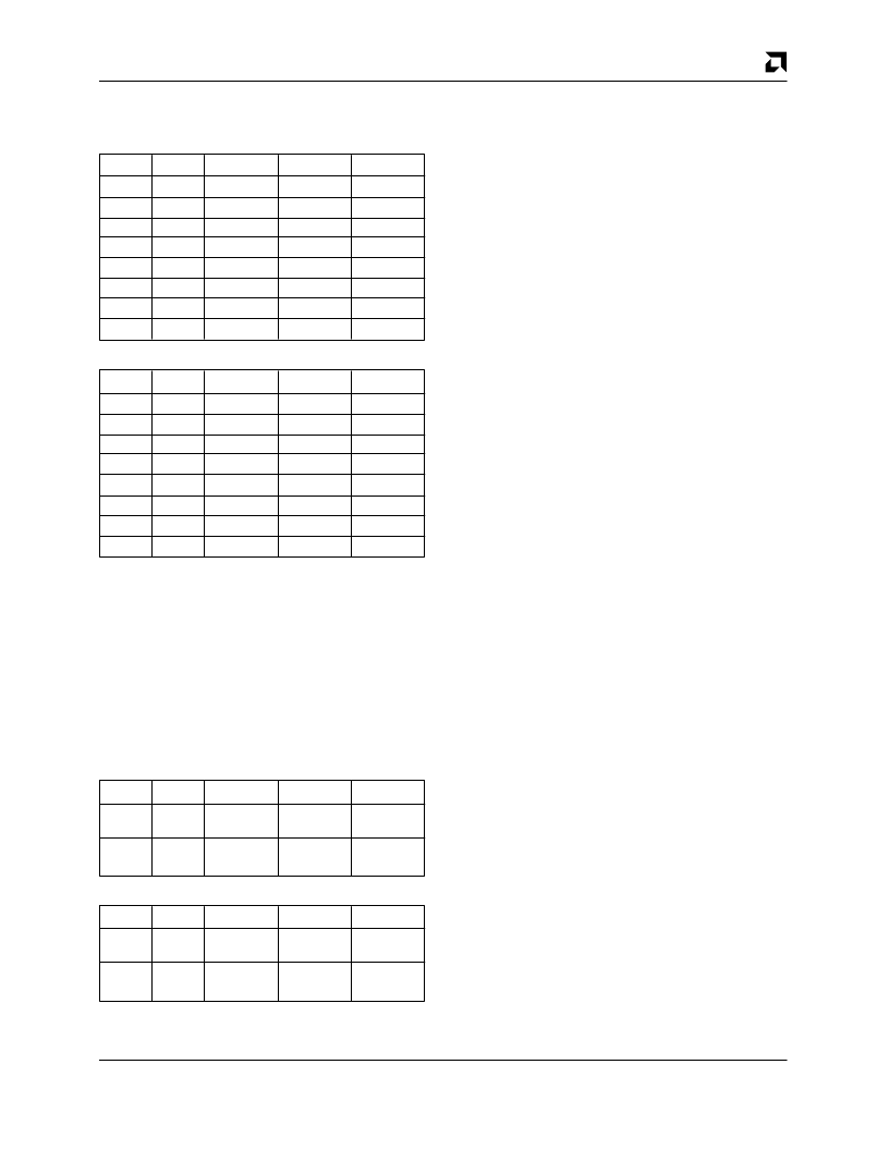
Byte Alignment For FIFO Read Operations
BE0
0
0
1
1
0
0
1
1
BE1
0
1
0
1
0
1
0
1
BSWP
0
0
0
0
1
1
1
1
DBUS7–0
n
n
n
X
n+1
n
n
X
DBUS15–8
n+1
n
n
X
n
n
n
X
Byte Alignment For FIFO Write Operations
BE0
0
0
1
1
0
0
1
1
BE1
0
1
0
1
0
1
0
1
BSWP
0
0
0
0
1
1
1
1
DBUS7–0
n
n
X
X
n+1
X
n
X
DBUS15–8
n+1
X
n
X
n
n
X
X
BIU to Control and Status
Register Data Path
All registers in the address range 2–31 are 8-bits wide.
When a read cycle is executed on any of these registers,
the MACE device will drive data on both bytes of the
data bus, regardless of the programming of BSWP.
When a write cycle is executed, the MACE device
strobes in data based on the programming of BSWP as
shown in the tables below. All accesses to addresses
2–31 are independent of the
BE
0
and
BE
1
pins.
Byte Alignment For Register Read Operations
BE0
X
BE1
X
BSWP
0
DBUS7–0
Read
Data
Read
Data
DBUS15–8
Read
Data
Read
Data
X
X
1
Byte Alignment For Register Write Operations
BE0
X
BE1
X
BSWP
0
DBUS7–0
Write
Data
X
DBUS15–8
X
Write
Data
X
X
1
FIFO Sub-System
The MACE device has two independent FIFOs, with
128-bytes for receive and 136-bytes for transmit opera-
tions. The FIFO sub-system contains both the FIFOs,
and the control logic to handle normal and exception re-
lated conditions.
The Transmit and Receive FIFOs interface on the net-
work side with the serializer/de-serializer in the MAC en-
gine. The BIU provides access between the FIFOs and
the host system to enable the movement of data to and
from the network.
Internally, the FIFOs appear to the BIU as independent
16-bit wide registers. Bytes or words can be written to
the Transmit FIFO (XMTFIFO), or read from the Re-
ceive FIFO (RCVFIFO). Byte and word transfers can be
mixed in any order. The BIU will ensure correct byte or-
dering dependent on the target host system, as deter-
mined by the programming of the BSWP bit in the BIU
Configuration Control register.
The XMTFIFO and RCVFIFO have three different
modes of operation. These are Normal (Default), Burst
and Low Latency Receive. Default operation will be
used after the hardware
RESET
pin or software SWRST
bit have been activated. The remainder of this general
description applies to all modes except where specific
differences are noted.
Transmit FIFO—General Operation:
When writing bytes to the XMTFIFO, certain restrictions
apply. These restrictions have a direct influence on the
latency provided by the FIFO to the host system. When
a byte is written to the FIFO location, the entire word lo-
cation is used. The unused byte is marked as a holein
the XMTFIFO. These holesare skipped during the seri-
alization process performed by the MAC engine, when
the bytes are unloaded from the XMTFIFO.
For instance, assume the Transmit FIFO Watermark
(XMTFW) is set for 32 write cycles. If the host writes byte
wide data to the XMTFIFO, after 36 write cycles there
will be space left in the XMTFIFO for only 32 more write
cycles. Therefore
TDTREQ
will de-assert even though
only 36-bytes of data have been loaded into the
XMTFIFO. Transmission will not commence until
64-bytes or the End-of-Frameare available in the
XMFIFO, so transmission would not start, and
TDTREQ
would remain de-asserted. Hence for byte wide data
transfers, the XMTFW should be programmed to the 8
or 16 write cycle limit, or the host should ensure that suf-
ficient data will be written to the XMTFIFO after
TDTREQ
has been de-asserted (which is permitted), to
guarantee that the transmission will commence. A third
alternative is to program the Transmit Start Point
(XMTSP) in the BIU Configuration Control register to
below the 64-byte default; thereby imposing a lower la-
tency to the host system requiring additional data to
相關(guān)PDF資料 |
PDF描述 |
|---|---|
| AM79C940 | Media Access Controller for Ethernet (MACE) |
| AM79C940JCW | Media Access Controller for Ethernet (MACE) |
| AM79C940KCW | Media Access Controller for Ethernet (MACE) |
| AM79C960 | PCnetTM-ISA Single-Chip Ethernet Controller |
| AM79C960KC | PCnetTM-ISA Single-Chip Ethernet Controller |
相關(guān)代理商/技術(shù)參數(shù) |
參數(shù)描述 |
|---|---|
| AM79C940VI | 制造商:未知廠家 制造商全稱:未知廠家 功能描述:LAN Node Controller |
| AM79C940VI/W | 制造商:未知廠家 制造商全稱:未知廠家 功能描述:LAN Node Controller |
| AM79C945 | 制造商:未知廠家 制造商全稱:未知廠家 功能描述: |
| AM79C945-16 | 制造商:未知廠家 制造商全稱:未知廠家 功能描述: |
| AM79C945-16JC | 制造商:未知廠家 制造商全稱:未知廠家 功能描述:LAN Node Controller |
發(fā)布緊急采購(gòu),3分鐘左右您將得到回復(fù)。