- 您現(xiàn)在的位置:買賣IC網(wǎng) > PDF目錄375289 > AM29BDS320GBD4VMI (SPANSION LLC) 32 Megabit (2 M x 16-Bit), 1.8 Volt-only Simultaneous Read/Write, Burst Mode Flash Memory PDF資料下載
參數(shù)資料
| 型號(hào): | AM29BDS320GBD4VMI |
| 廠商: | SPANSION LLC |
| 元件分類: | DRAM |
| 英文描述: | 32 Megabit (2 M x 16-Bit), 1.8 Volt-only Simultaneous Read/Write, Burst Mode Flash Memory |
| 中文描述: | 2M X 16 FLASH 1.8V PROM, 70 ns, PBGA64 |
| 封裝: | 8 X 9 MM, 0.80 MM PITCH, FBGA-64 |
| 文件頁數(shù): | 14/74頁 |
| 文件大?。?/td> | 701K |
| 代理商: | AM29BDS320GBD4VMI |
第1頁第2頁第3頁第4頁第5頁第6頁第7頁第8頁第9頁第10頁第11頁第12頁第13頁當(dāng)前第14頁第15頁第16頁第17頁第18頁第19頁第20頁第21頁第22頁第23頁第24頁第25頁第26頁第27頁第28頁第29頁第30頁第31頁第32頁第33頁第34頁第35頁第36頁第37頁第38頁第39頁第40頁第41頁第42頁第43頁第44頁第45頁第46頁第47頁第48頁第49頁第50頁第51頁第52頁第53頁第54頁第55頁第56頁第57頁第58頁第59頁第60頁第61頁第62頁第63頁第64頁第65頁第66頁第67頁第68頁第69頁第70頁第71頁第72頁第73頁第74頁
12
Am29BDS320G
27243B1 October 1, 2003
P r e l i m i n a r y
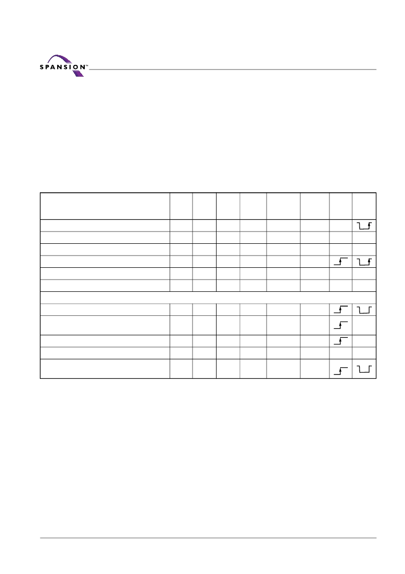
Device Bus Operations
This section describes the requirements and use of the device bus operations,
which are initiated through the internal command register. The command register
itself does not occupy any addressable memory location. The register is com-
posed of latches that store the commands, along with the address and data
information needed to execute the command. The contents of the register serve
as inputs to the internal state machine. The state machine outputs dictate the
function of the device. Table 1 lists the device bus operations, the inputs and con-
trol levels they require, and the resulting output. The following subsections
describe each of these operations in further detail.
Table 1. Device Bus Operations
Legend:
L = Logic 0, H = Logic 1, X = Don’t Care, S = Stable Logic 0 or 1 but no transitions.
Note:
Default active edge of CLK is the rising edge.
Enhanced VersatileIO (V
IO
) Control
The Enhanced VersatileIO (V
IO
) control allows the host system to set the voltage
levels that the device generates at its data outputs and the voltages tolerated at
its data and address inputs to the same voltage level that is asserted on the V
IO
pin. The device is available with either 1.65–1.95 or 2.7–3.15 V
IO
. This allows the
device to operate in 1.8 V or 3 V system environments as required.
For example, a V
IO
of 2.7 – 3.15 volts allows for I/O at the 3 volt level, driving
and receiving signals to and from other 3 V devices on the same bus.
Requirements for Asynchronous Read
Operation (Non-Burst)
To read data from the memory array, the system must first assert a valid address
on A20–A0, while driving AVD# and CE# to V
IL
. WE# should remain at V
IH
. The
rising edge of AVD# latches the address. The data will appear on DQ15–DQ0.
Operation
CE#
OE#
W E#
A20–0
DQ15– 0
RESET#
CLK
( See
Note)
AVD#
Asynchronous Read - Addresses Latched
L
L
H
Addr In
I/O
H
X
Asynchronous Read - Addresses Steady State
L
L
H
Addr In
I/O
H
X
L
Asynchronous Write
L
H
L
Addr In
I/O
H
L
L
Synchronous Write
L
H
L
Addr In
I/O
H
Standby (CE#)
H
X
X
HIGH Z
HIGH Z
H
X
X
Hardware Reset
X
X
X
HIGH Z
HIGH Z
L
X
X
Burst Read Operations
Load Starting Burst Address
L
X
H
Addr In
X
H
Advance Burst to next address with
appropriate Data presented on the Data Bus
L
L
H
HIGH Z
Burst
Data Out
H
H
Terminate current Burst read cycle
H
X
H
HIGH Z
HIGH Z
H
X
Terminate current Burst read cycle via RESET#
X
X
H
HIGH Z
HIGH Z
L
X
X
Terminate current Burst read cycle and start
new Burst read cycle
L
X
H
HIGH Z
I/O
H
相關(guān)PDF資料 |
PDF描述 |
|---|---|
| AM29BDS320GBD8VMI | 32 Megabit (2 M x 16-Bit), 1.8 Volt-only Simultaneous Read/Write, Burst Mode Flash Memory |
| AM29BDS320GBD9VMI | 32 Megabit (2 M x 16-Bit), 1.8 Volt-only Simultaneous Read/Write, Burst Mode Flash Memory |
| AM29BDS320GTC4VMI | 32 Megabit (2 M x 16-Bit), 1.8 Volt-only Simultaneous Read/Write, Burst Mode Flash Memory |
| AM29BDS320GTC8VMI | 32 Megabit (2 M x 16-Bit), 1.8 Volt-only Simultaneous Read/Write, Burst Mode Flash Memory |
| AM29BDS320GTC9VMI | 32 Megabit (2 M x 16-Bit), 1.8 Volt-only Simultaneous Read/Write, Burst Mode Flash Memory |
相關(guān)代理商/技術(shù)參數(shù) |
參數(shù)描述 |
|---|---|
| AM29BDS643GT5KVAI | 制造商:Spansion 功能描述:FLASH PARALLEL 1.8V 64MBIT 4MX16 55NS 44FBGA - Trays |
| AM29BL802CB-65RZET | 制造商:Spansion 功能描述: |
| AM29C01WW WAF | 制造商:Advanced Micro Devices 功能描述: |
| AM29C10API | 制造商:Rochester Electronics LLC 功能描述:- Bulk |
| AM29C10AWW DIE | 制造商:Advanced Micro Devices 功能描述: |
發(fā)布緊急采購,3分鐘左右您將得到回復(fù)。