- 您現(xiàn)在的位置:買賣IC網(wǎng) > PDF目錄375269 > ADV7314 (Analog Devices, Inc.) Multiformat 216 MHz Video Encoder with Six NSV 14-Bit DACs PDF資料下載
參數(shù)資料
| 型號: | ADV7314 |
| 廠商: | Analog Devices, Inc. |
| 英文描述: | Multiformat 216 MHz Video Encoder with Six NSV 14-Bit DACs |
| 中文描述: | 多格式視頻編碼器216兆赫六噪聲整形的14位DAC |
| 文件頁數(shù): | 32/84頁 |
| 文件大小: | 1069K |
| 代理商: | ADV7314 |
第1頁第2頁第3頁第4頁第5頁第6頁第7頁第8頁第9頁第10頁第11頁第12頁第13頁第14頁第15頁第16頁第17頁第18頁第19頁第20頁第21頁第22頁第23頁第24頁第25頁第26頁第27頁第28頁第29頁第30頁第31頁當(dāng)前第32頁第33頁第34頁第35頁第36頁第37頁第38頁第39頁第40頁第41頁第42頁第43頁第44頁第45頁第46頁第47頁第48頁第49頁第50頁第51頁第52頁第53頁第54頁第55頁第56頁第57頁第58頁第59頁第60頁第61頁第62頁第63頁第64頁第65頁第66頁第67頁第68頁第69頁第70頁第71頁第72頁第73頁第74頁第75頁第76頁第77頁第78頁第79頁第80頁第81頁第82頁第83頁第84頁
REV. 0
–32–
ADV7314
Simultaneous Standard Definition and
Progressive Scan or HDTV
Address [01h]: Input Mode 011(SD 40-Bit, PS 20-Bit) or
101 (SH and HD, SD Oversampled), 110 (SD and HD, HD
Oversampled)
YCrCb PS, HDTV, or any other HD data must be input in
4:2:2 format. In 4:2:2 input mode, the HD Y data is input on
Pins Y9–Y0 and the HD CrCb data on C9–C0.
If PS 4:2:2 data is interleaved onto a single 10-bit bus, Y9–Y0 are
used for the input port. The input data is to be input at 27 MHz
with the data clocked on the rising and falling edge of the input
clock. The input mode register at Address 01h is set accordingly.
If the YCrCb data does not conform to SMPTE 293M (525p),
ITU-R BT.1358M (625p), SMPTE 274M (1080i), SMPTE
296M (720p), or BTA T-1004, the Async Timing mode must
be used.
The 8-bit or 10-bit standard definition data must be compliant
to ITU-R BT.601/656 in 4:2:2 format.
Standard definition data is input on Pins S9–S0, with S0 being the
LSB. Using 8-bit input format, the data is input on Pins S9–S2.
The clock input for SD must be input on CLKIN_A, and the
clock input for HD must be input on CLKIN_B.
Synchronization signals are optional. SD syncs are input on pins
S_VSYNC
,
S_ HSYNC
, and
S_BLANK
.
HD syncs are input on Pins
P_VSYNC
,
P_ HSYNC
,
P_BLANK
.
S_VSYNC
S_HSYNC
S_BLANK
CLKIN_A
P_VSYNC
P_HSYNC
P_BLANK
CLKIN_B
MPEG2
DECODER
3
27MHz
10
YCrCb
INTERLACED TO
PROGRESSIVE
10
CrCb
10
Y
3
27MHz
S[9:0]
C[9:0]
Y[9:0]
ADV7314
Figure 23. Simultaneous PS and SD Input
S_VSYNC
S_HSYNC
S_BLANK
CLKIN_A
P_VSYNC
P_HSYNC
P_BLANK
CLKIN_B
SDTV
DECODER
3
27MHz
10
YCrCb
HDTV
DECODER
10
CrCb
10
Y
3
74.25MHz
1080 i
720 p
S[9:0]
C[9:0]
Y[9:0]
ADV7314
Figure 24. Simultaneous HD and SD Input
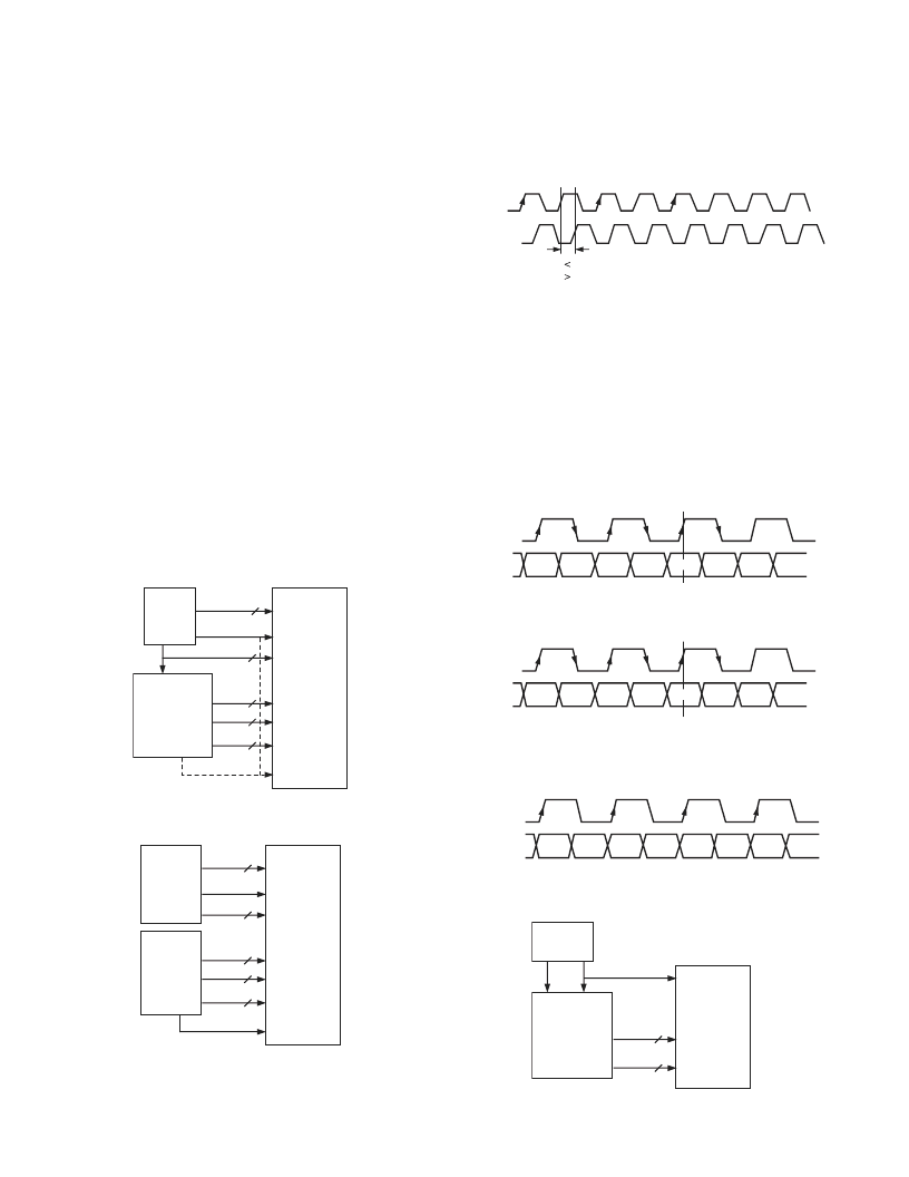
If in simultaneous SD/HD input mode, the two clock phases
differ by less than 9.25 ns or more than 27.75 ns, the CLOCK
ALIGN bit [Address 01h, Bit 3] must be set accordingly. If the
application uses the same clock source for both SD and PS, the
CLOCK ALIGN bit must be set since the phase difference
between both inputs is less than 9.25 ns.
t
DELAY
t
DELAY
9.25ns OR
27.75ns
CLKIN_A
CLKIN_B
Figure 25. Clock Phase with Two Input Clocks
Progressive Scan at 27 MHz (Dual Edge) or 54 MHz
Address [01h]: Input Mode 100 OR 111, Respectively
YCrCb progressive scan data can be input at 27 MHz or 54
MHz. The input data is interleaved onto a single 8-/10-bit bus
and is input on Pins Y9–Y0. When a 27 MHz clock is supplied,
the data is clocked in on the rising and falling edge of the input
clock and CLOCK EDGE [Address 01h, Bit 1] must be set
accordingly.
The following figures show the possible conditions. (a) Cb data
on the rising edge and (b) Y data on the rising edge.
3FF
00
00
XY
Y0
Y1
Cr0
CLKIN_B
Y9–Y0
Cb0
Figure 26a. Clock Edge Address 01h, Bit 1
Should Be Set to 0
3FF
00
00
XY
Cb0
Cr0
Y1
CLKIN_B
Y9–Y0
Y0
Figure 26b. Clock Edge Address 01h, Bit 1
Should Be Set to 1
With a 54 MHz clock, the data is latched on the every rising edge.
PIXEL INPUT
DATA
3FF
00
00
XY
Cb0
Y0
Y1
Cr0
CLKIN
Figure 26c. Input Sequence in PS Bit Interleaved
Mode, EAV/SAV Followed by Cb0 Data
MPEG2
DECODER
P_VSYNC
P_HSYNC
P_BLANK
CLKIN_A
Y[9:0]
INTERLACED
TO
PROGRESSIVE
YCrCb
10
3
27MHz OR
54MHz
YCrCb
ADV7314
Figure 27. 1 10-Bit PS at 27 MHz or 54 MHz
相關(guān)PDF資料 |
PDF描述 |
|---|---|
| ADV7314KST | Multiformat 216 MHz Video Encoder with Six NSV 14-Bit DACs |
| ADV7322 | Multiformat 11-Bit HDTV Video Encoder |
| ADV7322KSTZ1 | Multiformat 11-Bit HDTV Video Encoder |
| ADV7400 | ADV7402/ADV7400 Multiformat Video Decoders for Advanced TV |
| ADV7400KST-110 | ADV7402/ADV7400 Multiformat Video Decoders for Advanced TV |
相關(guān)代理商/技術(shù)參數(shù) |
參數(shù)描述 |
|---|---|
| ADV7314KST | 制造商:AD 制造商全稱:Analog Devices 功能描述:Multiformat 216 MHz Video Encoder with Six NSV 14-Bit DACs |
| ADV73186702 | 制造商:LG Corporation 功能描述:FRAME ASSEMBLY,DOOR |
| ADV73186703 | 制造商:LG Corporation 功能描述:FRAME ASSEMBLY,DOOR |
| ADV7320 | 制造商:AD 制造商全稱:Analog Devices 功能描述:Multiformat 216 MHz Video Encoder with Six NSV 12-Bit DACs |
| ADV73205705 | 制造商:LG Corporation 功能描述:Frame Assembly |
發(fā)布緊急采購,3分鐘左右您將得到回復(fù)。