- 您現(xiàn)在的位置:買(mǎi)賣(mài)IC網(wǎng) > PDF目錄374047 > ADV7190KST (ANALOG DEVICES INC) Video Encoder with Six 10-Bit DACs and Video Encoder with Six DAC Outputs PDF資料下載
參數(shù)資料
| 型號(hào): | ADV7190KST |
| 廠(chǎng)商: | ANALOG DEVICES INC |
| 元件分類(lèi): | 顏色信號(hào)轉(zhuǎn)換 |
| 英文描述: | Video Encoder with Six 10-Bit DACs and Video Encoder with Six DAC Outputs |
| 中文描述: | COLOR SIGNAL ENCODER, PQFP64 |
| 封裝: | LQFP-64 |
| 文件頁(yè)數(shù): | 38/69頁(yè) |
| 文件大小: | 628K |
| 代理商: | ADV7190KST |
第1頁(yè)第2頁(yè)第3頁(yè)第4頁(yè)第5頁(yè)第6頁(yè)第7頁(yè)第8頁(yè)第9頁(yè)第10頁(yè)第11頁(yè)第12頁(yè)第13頁(yè)第14頁(yè)第15頁(yè)第16頁(yè)第17頁(yè)第18頁(yè)第19頁(yè)第20頁(yè)第21頁(yè)第22頁(yè)第23頁(yè)第24頁(yè)第25頁(yè)第26頁(yè)第27頁(yè)第28頁(yè)第29頁(yè)第30頁(yè)第31頁(yè)第32頁(yè)第33頁(yè)第34頁(yè)第35頁(yè)第36頁(yè)第37頁(yè)當(dāng)前第38頁(yè)第39頁(yè)第40頁(yè)第41頁(yè)第42頁(yè)第43頁(yè)第44頁(yè)第45頁(yè)第46頁(yè)第47頁(yè)第48頁(yè)第49頁(yè)第50頁(yè)第51頁(yè)第52頁(yè)第53頁(yè)第54頁(yè)第55頁(yè)第56頁(yè)第57頁(yè)第58頁(yè)第59頁(yè)第60頁(yè)第61頁(yè)第62頁(yè)第63頁(yè)第64頁(yè)第65頁(yè)第66頁(yè)第67頁(yè)第68頁(yè)第69頁(yè)
ADV7190/ADV7191
–38–
REV. 0
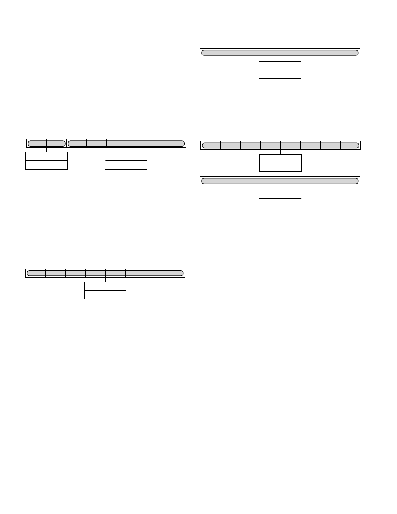
CGMS_WSS REGISTER 1 C/W1 (C/W17–C/W10)
(Address (SR4–SR0) = 1AH)
CGMS_WSS Register 1 is an 8-bit-wide register. Figure 70 shows
the operations under control of this register.
C/W1 BIT DESCRIPTION
CGMS/WSS Data (C/W10–C/W15)
These bit locations are shared by CGMS data and WSS data. In
NTSC mode these bits are CGMS data. In PAL mode these bits
are WSS data.
CGMS Data (C/W16–C/W17)
These bits are CGMS data bits only.
C/W17
C/W16
C/W15
C/W14
C/W13
C/W12
C/W11
C/W10
C/W15
–
C/W10
CGMS/WSS DATA
C/W17
–
C/W16
CGMS DATA
Figure 70. CGMS_WSS Register 1
CGMS_WSS REGISTER 2
C/W1 (C/W27–C/W20)
(Address (SR4–SR0) = 1BH)
CGMS_WSS Register 2 is an 8-bit-wide register. Figure 71 shows
the operations under control of this register.
C/W2 BIT DESCRIPTION
CGMS/WSS Data (C/W20–C/W27)
These bit locations are shared by CGMS data and WSS data. In
NTSC mode these bits are CGMS data. In PAL mode these bits
are WSS data.
C/W27
–
C/W20
CGMS/WSS DATA
C/W27
C/W26
C/W25
C/W24
C/W23
C/W22
C/W21
C/W20
Figure 71. CGMS_WSS Register 2
CONTRAST CONTROL REGISTER (CC00–CC07)
(Address (SR4–SR0) = 1DH)
The contrast control register is an 8-bit-wide register used to
scale the Y output levels. Figure 72 shows the operation under
control of this register.
Y Scale Value (CC00–CC07)
These eight bits represent the value required to scale the Y pixel
data from 0.0 to 1.5 of its initial level. The value of these eight
bits is calculated using the following equation:
Y Scale Value
=
Scale Factor
×
128
Example:
Scale Factor = 1.18
Y Scale Value = 1.18
×
128 = 151.04
Y Scale Value = 151 (rounded to the nearest integer)
Y Scale Value = 10010111
b
Y Scale Value = 97
h
CC07
–
CC00
Y SCALE VALUE
CC07
CC06
CC05
CC04
CC03
CC02
CC01
CC00
Figure 72. Contrast Control Register
COLOR CONTROL REGISTERS 2–1 (CC2–CC1)
(Address (SR4–SR0) = 1EH–1FH)
The color control registers are 8-bit-wide registers used to scale
the U and V output levels. Figure 73 shows the operations under
control of these registers.
CC17
–
CC10
U SCALE VALUE
CC17
CC16
CC15
CC14
CC13
CC12
CC11
CC10
CC27
–
CC20
V SCALE VALUE
CC27
CC26
CC25
CC24
CC23
CC22
CC21
CC20
Figure 73. Color Control Registers
CC1 BIT DESCRIPTION
U Scale Value (CC10–CC17)
These eight bits represent the value required to scale the U level
from 0.0 to 2.0 of its initial level. The value of these eight bits is
calculated using the following equation:
U Scale Value
=
Scale Factor
×
128
Example:
Scale Factor = 1.18
U Scale Value = 1.18
×
128 = 151.04
U Scale Value = 151 (rounded to the nearest integer)
U Scale Value = 10010111
b
U Scale Value = 97
h
CC2 BIT DESCRIPTION
V Scale Value (CC20–CC27)
These eight bits represent the value required to scale the V pixel
data from 0.0 to 2.0 of its initial level. The value of these eight
bits is calculated using the following equation:
V Scale Value
=
Scale Factor
×
128
Example:
Scale Factor = 1.18
V Scale Value = 1.18
×
128 = 151.04
V Scale Value = 151 (rounded to the nearest integer)
V Scale Value = 10010111
b
V Scale Value = 97
h
相關(guān)PDF資料 |
PDF描述 |
|---|---|
| ADV7191 | Video Encoder with Six 10-Bit DACs and Video Encoder with Six DAC Outputs |
| ADV7191KST | Video Encoder with Six 10-Bit DACs and Video Encoder with Six DAC Outputs |
| ADV7190 | Video Encoder with Six 10-Bit DACs and Video Encoder with Six DAC Outputs |
| ADV7192KST | Video Encoder with Six 10-Bit DACs, 54 MHz Oversampling and Progressive Scan Inputs |
| ADV7192 | Video Encoder with Six 10-Bit DACs, 54 MHz Oversampling and Progressive Scan Inputs |
相關(guān)代理商/技術(shù)參數(shù) |
參數(shù)描述 |
|---|---|
| ADV7190KSTZ | 制造商:Analog Devices 功能描述:Video Encoder 6DAC 10-Bit 64-Pin LQFP |
| ADV7191 | 制造商:AD 制造商全稱(chēng):Analog Devices 功能描述:Video Encoder with Six 10-Bit DACs and Video Encoder with Six DAC Outputs |
| ADV7191KST | 制造商:Analog Devices 功能描述:Video Encoder 6DAC 10-Bit 64-Pin LQFP 制造商:Rochester Electronics LLC 功能描述:54M 4X STD DEF ENCODER NON-MACRO I.C. - Tape and Reel |
| ADV7191KSTZ | 制造商:Analog Devices 功能描述:Video Encoder 6DAC 10-Bit 64-Pin LQFP 制造商:Analog Devices 功能描述:IC VIDEO ENCODER |
| ADV7192 | 制造商:AD 制造商全稱(chēng):Analog Devices 功能描述:Video Encoder with Six 10-Bit DACs, 54 MHz Oversampling and Progressive Scan Inputs |
發(fā)布緊急采購(gòu),3分鐘左右您將得到回復(fù)。