- 您現(xiàn)在的位置:買賣IC網(wǎng) > PDF目錄374044 > ADV601 (Analog Devices, Inc.) Low Cost Multiformat Video Codec PDF資料下載
參數(shù)資料
| 型號(hào): | ADV601 |
| 廠商: | Analog Devices, Inc. |
| 元件分類: | 視頻Codec |
| 英文描述: | Low Cost Multiformat Video Codec |
| 中文描述: | 低成本多格式視頻解碼器 |
| 文件頁數(shù): | 49/52頁 |
| 文件大小: | 606K |
| 代理商: | ADV601 |
第1頁第2頁第3頁第4頁第5頁第6頁第7頁第8頁第9頁第10頁第11頁第12頁第13頁第14頁第15頁第16頁第17頁第18頁第19頁第20頁第21頁第22頁第23頁第24頁第25頁第26頁第27頁第28頁第29頁第30頁第31頁第32頁第33頁第34頁第35頁第36頁第37頁第38頁第39頁第40頁第41頁第42頁第43頁第44頁第45頁第46頁第47頁第48頁當(dāng)前第49頁第50頁第51頁第52頁
ADV601
–49–
REV. 0
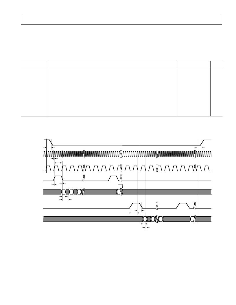
DSP Interface Timing
The diagram in this section shows transfer timing for one set of video statistics and calculated bin widths as they pass through the
ADV601’s DSP interface. Whenever an ADV601’s serial port is inactive, the codec’s TXD pin is three-stated and the codec ignores
the state of the RXD pin. Figure 41 illustrates the ADV601 serial interface’s signal, sample and frame relationships for the transmit
and receive modes.
Table XXXVII. DSP Read and Write Transfer Timing Parameters
Parameter
Description
Min
Max
Unit
t
TCLK_DIRQ_D
t
TCLK_DIRQ_OH
t
VCLK_TCLK_D
t
TCLK_TF_D
t
TCLK_TF_OH
t
TCLK_TXD_D
t
TCLK_TXD_OH
t
TCLK_RF_S
t
TCLK_RF_H
t
TCLK_RXD_S
t
TCLK_RXD_H
DIRQ
Signal, Transfer-Receive Cycle Start, Delay
DIRQ
Signal, Transfer-Receive Cycle End, Output Hold
TCLK
Signal, Referenced to VCLK, Delay
TF Signal, Transfer Frame Reference to TCLK, Delay
TF Signal, Transfer Frame Reference to TCLK, Output Hold
TXD Sample, Transfer Data, Delay (at 27 MHz VCLK)
TXD Sample, Transfer Data, Output Hold
RF Signal, Receive Frame Referenced to TCLK, Setup
RF Signal, Receive Frame Referenced to TCLK, Hold
RXD Sample, Receive Data, Setup
RXD Sample, Receive Data, Hold (at 27 MHz VCLK)
N/A
3
N/A
N/A
2
N/A
2
2
105
2
16.8
2
4
N/A
11
3
N/A
24.2
1
N/A
N/A
N/A
N/A
N/A
ns
ns
ns
ns
ns
ns
ns
ns
ns
ns
ns
NOTES
1
Maximum t
TCLK_TXD_D
varies with VCLK according to the formula: t
TCLK_TXD_D
(MAX)
= 0.5 (VCLK Period) +4.7.
2
Minimum t
TCLK_RXD_H
varies with VCLK according to the formula: t
TCLK_RXD_H
(MIN)
= 1.5 (VCLK Period) –36.
(O)
DIRQ
DSP CALCULATES BIN WIDTHS
FROM VIDEO STATISTICS
(I) VCLK
(O) TCLK
TCLK PERIOD = 4
·
VCLK PERIOD
FIFTY-TWO 16-BIT WORDS TRANSFERRED BY THE ADV601
-- ADV601 REGISTERS 0x06 AND 0x80 THROUGH 0xB2
EIGHTY-FOUR 16-BIT WORDS TRANSFERRED BY THE DSP
-- ADV601 REGISTERS 0x100 THROUGH 0x153
(O) TF
(O) TXD
t
TCLK_TXD_OH
TCLK_TXD_D
t
TCLK_RF_S
t
TCLK_RXD_H
t
TCLK_RXD_S
(I) RF
(I) RXD
t
TCLK_DIRQ_OH
t
TCLK_DIRQ_D
t
TCLK_TF_D
t
VCLK_TCLK_D
t
TCLK_RF_H
t
TCLK_TF_OH
Figure 41. DSP Read and Write Transfer Timing
相關(guān)PDF資料 |
PDF描述 |
|---|---|
| ADV601JS | Low Cost Multiformat Video Codec |
| ADV601LC | Ultralow Cost Video Codec |
| ADV601LCJST | Ultralow Cost Video Codec |
| ADV7120KP30 | CMOS 80 MHz, Triple 8-Bit Video DAC |
| ADV7120 | CMOS 80 MHz, Triple 8-Bit Video DAC |
相關(guān)代理商/技術(shù)參數(shù) |
參數(shù)描述 |
|---|---|
| ADV601E-VIDEOPIPE | 制造商:Analog Devices 功能描述:VIDEOPIPE |
| ADV601JS | 制造商:Analog Devices 功能描述:Multiformat Video Codec 160-Pin MQFP 制造商:Rochester Electronics LLC 功能描述:- Bulk |
| ADV601JS12 | 制造商:Analog Devices 功能描述:Multiformat Video Codec 160-Pin MQFP 制造商:Rochester Electronics LLC 功能描述:DIGITAL VIDEO CODEC REV 1.2 - Bulk |
| ADV601LC | 制造商:AD 制造商全稱:Analog Devices 功能描述:Ultralow Cost Video Codec |
| ADV601LCERAG1266B-0.5 | 制造商:Analog Devices 功能描述: |
發(fā)布緊急采購,3分鐘左右您將得到回復(fù)。