- 您現(xiàn)在的位置:買賣IC網(wǎng) > PDF目錄374016 > ADMCF340-EVALKIT (Analog Devices, Inc.) Circular Connector; No. of Contacts:7; Series:MS27497; Body Material:Aluminum; Connecting Termination:Crimp; Connector Shell Size:10; Circular Contact Gender:Pin; Circular Shell Style:Wall Mount Receptacle; Insert Arrangement:10-99 RoHS Compliant: No PDF資料下載
參數(shù)資料
| 型號: | ADMCF340-EVALKIT |
| 廠商: | Analog Devices, Inc. |
| 元件分類: | 圓形連接器 |
| 英文描述: | Circular Connector; No. of Contacts:7; Series:MS27497; Body Material:Aluminum; Connecting Termination:Crimp; Connector Shell Size:10; Circular Contact Gender:Pin; Circular Shell Style:Wall Mount Receptacle; Insert Arrangement:10-99 RoHS Compliant: No |
| 中文描述: | DashDSPTM 64無鉛閃存混合信號增強(qiáng)的DSP與模擬前端 |
| 文件頁數(shù): | 21/40頁 |
| 文件大?。?/td> | 415K |
| 代理商: | ADMCF340-EVALKIT |
第1頁第2頁第3頁第4頁第5頁第6頁第7頁第8頁第9頁第10頁第11頁第12頁第13頁第14頁第15頁第16頁第17頁第18頁第19頁第20頁當(dāng)前第21頁第22頁第23頁第24頁第25頁第26頁第27頁第28頁第29頁第30頁第31頁第32頁第33頁第34頁第35頁第36頁第37頁第38頁第39頁第40頁
REV. 0
ADMCF340
–21–
V
C
V1
PWMSYNC
COMPARATOR
OUTPUT
V
CMAX
T
VIL
T
PWM
– T
CRST
T
CRST
V
VIL
t
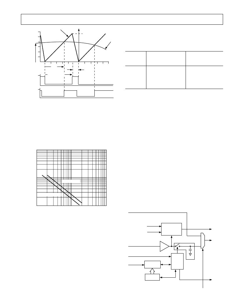
Figure 12. Analog Input Block Operation
The ADC system consists of four comparators and a single
timer that may be clocked at either the DSP rate or half the
DSP rate, depending on the setting of the ADCCNT bit (Bit 7)
of the MODECTRL Register. When this bit is cleared, the
timer counts at a slower rate of CLKIN. When this bit is set, the
timer counts at CLKOUT or twice the rate of CLKIN. ADC1,
ADC2, ADC3, and ADCAUX are the registers that capture the
conversion times, which are the timer values when the associ-
ated comparator trips.
100
10
1
1 10 100
C
N
TUNED I
CONST
DEFAULT I
CONST
Figure 13. Timing Capacitor Selection
ADC Resolution
The ADC is intrinsically linked to the PWM block through the
PWMSYNC pulse controlling the ADC conversion process.
Because of this link, the effective resolution of the ADC is a
function of both the PWM switching frequency and the rate at
which the ADC counter timer is clocked. For a CLKOUT
period of
T
CK
and a PWM period of
T
PWM
, the maximum count
of the ADC is given by:
=
(
Max Count
T
(
T
T
for MODECTRL Bit
(
Max Count
T
(
T
T
for MODECTRL Bit
PWM
CRST
=
7
CK
PWM
CRST
=
7
CK
)
)
=
)
)
min
,
/
min
,
/
4095
2
0
4095
1
Where
T
PWM
is equal to the PWM period if operating in single
update mode, or it is equal to half that period if operating in
double update mode. For an assumed CLKOUT frequency of
20 MHz and PWMSYNC pulsewidth of 2.0
μ
s, the effective
resolution of the ADC block is tabulated for various PWM
switching frequencies in Table VIII.
Table VIII. ADC Resolution Examples
PWM
Frequency
(kHz)
MODECTRL[7] = 0
Max
Count
MODECTRL[7] = 1
Max
Effective
Count
Resolution
Effective
Resolution
2.4
4
8
18
25
4095
2480
1230
535
380
12
>11
>10
>9
>8
4095
4095
2460
1070
760
12
12
>11
>10
>9
Programmable Current Source
The ADMCF340 has an internal current source that is used to
charge an external capacitor, generating the voltage ramp used for
conversion. The magnitude of the output of the current source circuit is
subject to manufacturing variations and can vary from one device to
the next. Therefore, the ADMCF340 includes a programmable
current source whose output can always be tuned to within 5% of
the target 100
μ
A. A 3-bit register, ICONST_TRIM, allows the
user to make this adjustment. The output current is proportional to
the value written to the register: 0x0 produces the minimum output,
and 0x7 produces the maximum output. The default value of
ICONST_TRIM after reset is 0x0.
Suggested implementations of the calibration routine are pro-
vided through Application Notes and code that can be found by
visiting www.analog.com/motorcontrol.
Charging Capacitor Selection
The charging capacitor value is selected based on the sample
(PWM) frequency desired. Too small a capacitor value will re-
duce the available resolution of the ADC by having the ramp voltage
rise rapidly and convert too quickly, not utilizing all possible counts
available in the PWM cycle. Too large a capacitor may not convert in
the available PWM cycle returning 0x000. To select a charging capaci-
tor, use Figure 13, select the sampling frequency desired, determine
if the current source is to be tuned to a nominal 100
μ
A or left in
the default (0x0 code) trim state, then determine the proper charge
capacitor off the appropriate curve.
SHA TIMER
REGISTER
SHA
STATE
MACHINE
M
OVERCURRENT
COMPARATOR
SHA TIMER
COUNTER
VOLTAGE
CURRENT
PWMSYNC
CLOCKOUT
MODECTRL REGISTER
CHANNEL SELECTION (I
SENSE
/V)
ADC CONVERSION
STATUS BIT
(ADC REGISTER)
SHA
–25x
VxL
(TO ADC)
TRIP
(TO PWMTRIP FILTER)
TRIP REF HIGH
TRIP REF LOW
Figure 14. Analog Front End Block Diagram
相關(guān)PDF資料 |
PDF描述 |
|---|---|
| ADMCF341 | DashDSP⑩ 28-Lead Flash Mixed-Signal DSP with Enhanced Analog Front End |
| ADMCF341BR | DashDSP⑩ 28-Lead Flash Mixed-Signal DSP with Enhanced Analog Front End |
| ADMCF341-EVALKIT | DashDSP⑩ 28-Lead Flash Mixed-Signal DSP with Enhanced Analog Front End |
| ADN2811 | OC-48/OC-48 FEC Clock and Data Recovery IC with Integrated Limiting Amp |
| ADN2811ACP-CML | OC-48/OC-48 FEC Clock and Data Recovery IC with Integrated Limiting Amp |
相關(guān)代理商/技術(shù)參數(shù) |
參數(shù)描述 |
|---|---|
| ADMCF340XSTB | 制造商:Analog Devices 功能描述: |
| ADMCF341 | 制造商:AD 制造商全稱:Analog Devices 功能描述:DashDSP⑩ 28-Lead Flash Mixed-Signal DSP with Enhanced Analog Front End |
| ADMCF341BR | 制造商:Analog Devices 功能描述:DSP Fixed-Point/Floating-Point 16-Bit 20MHz 20MIPS 28-Pin SOIC W T/R |
| ADMCF341BRZ-REEL | 制造商:Analog Devices 功能描述: |
| ADMCF341-EVALKIT | 制造商:AD 制造商全稱:Analog Devices 功能描述:DashDSP⑩ 28-Lead Flash Mixed-Signal DSP with Enhanced Analog Front End |
發(fā)布緊急采購,3分鐘左右您將得到回復(fù)。