- 您現(xiàn)在的位置:買(mǎi)賣(mài)IC網(wǎng) > PDF目錄374016 > ADMCF340-EVALKIT (Analog Devices, Inc.) Circular Connector; No. of Contacts:7; Series:MS27497; Body Material:Aluminum; Connecting Termination:Crimp; Connector Shell Size:10; Circular Contact Gender:Pin; Circular Shell Style:Wall Mount Receptacle; Insert Arrangement:10-99 RoHS Compliant: No PDF資料下載
參數(shù)資料
| 型號(hào): | ADMCF340-EVALKIT |
| 廠商: | Analog Devices, Inc. |
| 元件分類(lèi): | 圓形連接器 |
| 英文描述: | Circular Connector; No. of Contacts:7; Series:MS27497; Body Material:Aluminum; Connecting Termination:Crimp; Connector Shell Size:10; Circular Contact Gender:Pin; Circular Shell Style:Wall Mount Receptacle; Insert Arrangement:10-99 RoHS Compliant: No |
| 中文描述: | DashDSPTM 64無(wú)鉛閃存混合信號(hào)增強(qiáng)的DSP與模擬前端 |
| 文件頁(yè)數(shù): | 18/40頁(yè) |
| 文件大?。?/td> | 415K |
| 代理商: | ADMCF340-EVALKIT |
第1頁(yè)第2頁(yè)第3頁(yè)第4頁(yè)第5頁(yè)第6頁(yè)第7頁(yè)第8頁(yè)第9頁(yè)第10頁(yè)第11頁(yè)第12頁(yè)第13頁(yè)第14頁(yè)第15頁(yè)第16頁(yè)第17頁(yè)當(dāng)前第18頁(yè)第19頁(yè)第20頁(yè)第21頁(yè)第22頁(yè)第23頁(yè)第24頁(yè)第25頁(yè)第26頁(yè)第27頁(yè)第28頁(yè)第29頁(yè)第30頁(yè)第31頁(yè)第32頁(yè)第33頁(yè)第34頁(yè)第35頁(yè)第36頁(yè)第37頁(yè)第38頁(yè)第39頁(yè)第40頁(yè)
REV. 0
ADMCF340
–18–
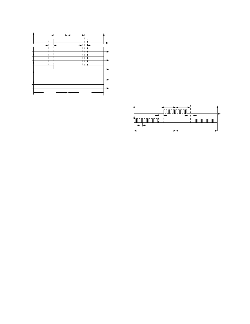
PWMCHA
= PWMCHB
PWMTM
PWMTM
AH
2 PWMDT
AL
BH
BL
2 PWMDT
CH
CL
Figure 9. An example of PWM signals suitable for ECM
control. PWMCHA = PWMCHB, BH/BL are a crossover
pair. AL, BH, CH, and CL outputs are disabled. Operation
is in single update mode.
Gate Drive Unit: PWMGATE Register
The gate drive unit of the PWM controller adds features that
simplify the design of isolated gate drive circuits for PWM
inverters. If a transformer-coupled power device gate drive amplifier is
used, the active PWM signal must be chopped at a high frequency.
The PWMGATE Register allows the programming of this high
frequency chopping mode. The chopped active PWM signals
may be required for the high side drivers only, for the low side
drivers only, or for both the high side and low side switches.
Therefore, independent control of this mode for both high side
and low side switches is included with two separate control bits
in the PWMGATE Register.
Typical PWM output signals with high frequency chopping
enabled on both high side and low side signals are shown in
Figure 10. Chopping of the high side PWM outputs (AH, BH,
and CH) is enabled by setting Bit 8 of the PWMGATE Register.
Chopping of the low side PWM outputs (AL, BL, and CL) is
enabled by setting Bit 9 of the PWMGATE Register. The high
chopping frequency is controlled by the 8-bit word (GDCLK)
written to Bits 0 to 7 of the PWMGATE Register. The period
and the frequency of this high frequency carrier are:
T
GDCLK
(
T
f
f
GDCLK
(
CHOP
CK
CHOP
CLKOUT
=
×
+
)
[
]
×
=
×
+
)
[
]
4
1
4
1
The
GDCLK
value may range from 0 to 255, corresponding
to a programmable chopping frequency rate from 19.5 kHz to
5 MHz for a 20 MHz CLKOUT rate. The gate drive features
must be programmed before operation of the PWM controller
and typically are not changed during normal operation of the
PWM controller. Following a reset, by default, all bits of the
PWMGATE Register are cleared so that high frequency
chopping is disabled.
PWMCHA PWMCHA
PWMTM
[4
(GDCLK + 1)
t
CK
]
PWMTM
2 PWMDT
2 PWMDT
Figure 10. Typical PWM signals with high frequency gate
chopping enabled on both high side and low side switches.
(GDCLK is the integer equivalent of the value in Bits 0 to
7 of the PWMGATE Register.)
PWM Polarity Control, PWMPOL Pin
The polarity of the PWM signals produced at the output pins
AH to CL may be selected in hardware by the PWMPOL Pin.
Connecting the PWMPOL Pin to DGND selects active LO PWM
outputs, such that a LO level is interpreted as a command to
turn on the associated power device. Conversely, connecting
the PWMPOL Pin to V
DD
selects active HI PWM and the asso-
ciated power devices are turned ON by a HI level at the PWM
outputs. There is an internal pull-up on the PWMPOL Pin, so
that if this pin becomes disconnected (or is not connected),
active HI PWM will be produced. The level on the PWMPOL
Pin may be read from Bit 2 of the SYSSTAT Register, where a
zero indicates a measured LO level at the PWMPOL Pin.
相關(guān)PDF資料 |
PDF描述 |
|---|---|
| ADMCF341 | DashDSP⑩ 28-Lead Flash Mixed-Signal DSP with Enhanced Analog Front End |
| ADMCF341BR | DashDSP⑩ 28-Lead Flash Mixed-Signal DSP with Enhanced Analog Front End |
| ADMCF341-EVALKIT | DashDSP⑩ 28-Lead Flash Mixed-Signal DSP with Enhanced Analog Front End |
| ADN2811 | OC-48/OC-48 FEC Clock and Data Recovery IC with Integrated Limiting Amp |
| ADN2811ACP-CML | OC-48/OC-48 FEC Clock and Data Recovery IC with Integrated Limiting Amp |
相關(guān)代理商/技術(shù)參數(shù) |
參數(shù)描述 |
|---|---|
| ADMCF340XSTB | 制造商:Analog Devices 功能描述: |
| ADMCF341 | 制造商:AD 制造商全稱(chēng):Analog Devices 功能描述:DashDSP⑩ 28-Lead Flash Mixed-Signal DSP with Enhanced Analog Front End |
| ADMCF341BR | 制造商:Analog Devices 功能描述:DSP Fixed-Point/Floating-Point 16-Bit 20MHz 20MIPS 28-Pin SOIC W T/R |
| ADMCF341BRZ-REEL | 制造商:Analog Devices 功能描述: |
| ADMCF341-EVALKIT | 制造商:AD 制造商全稱(chēng):Analog Devices 功能描述:DashDSP⑩ 28-Lead Flash Mixed-Signal DSP with Enhanced Analog Front End |
發(fā)布緊急采購(gòu),3分鐘左右您將得到回復(fù)。