- 您現(xiàn)在的位置:買賣IC網(wǎng) > PDF目錄374016 > ADMCF340-EVALKIT (Analog Devices, Inc.) Circular Connector; No. of Contacts:7; Series:MS27497; Body Material:Aluminum; Connecting Termination:Crimp; Connector Shell Size:10; Circular Contact Gender:Pin; Circular Shell Style:Wall Mount Receptacle; Insert Arrangement:10-99 RoHS Compliant: No PDF資料下載
參數(shù)資料
| 型號(hào): | ADMCF340-EVALKIT |
| 廠商: | Analog Devices, Inc. |
| 元件分類: | 圓形連接器 |
| 英文描述: | Circular Connector; No. of Contacts:7; Series:MS27497; Body Material:Aluminum; Connecting Termination:Crimp; Connector Shell Size:10; Circular Contact Gender:Pin; Circular Shell Style:Wall Mount Receptacle; Insert Arrangement:10-99 RoHS Compliant: No |
| 中文描述: | DashDSPTM 64無(wú)鉛閃存混合信號(hào)增強(qiáng)的DSP與模擬前端 |
| 文件頁(yè)數(shù): | 15/40頁(yè) |
| 文件大?。?/td> | 415K |
| 代理商: | ADMCF340-EVALKIT |
第1頁(yè)第2頁(yè)第3頁(yè)第4頁(yè)第5頁(yè)第6頁(yè)第7頁(yè)第8頁(yè)第9頁(yè)第10頁(yè)第11頁(yè)第12頁(yè)第13頁(yè)第14頁(yè)當(dāng)前第15頁(yè)第16頁(yè)第17頁(yè)第18頁(yè)第19頁(yè)第20頁(yè)第21頁(yè)第22頁(yè)第23頁(yè)第24頁(yè)第25頁(yè)第26頁(yè)第27頁(yè)第28頁(yè)第29頁(yè)第30頁(yè)第31頁(yè)第32頁(yè)第33頁(yè)第34頁(yè)第35頁(yè)第36頁(yè)第37頁(yè)第38頁(yè)第39頁(yè)第40頁(yè)
REV. 0
ADMCF340
–15–
which means that the width of the pulse is programmable from T
CK
to 256 T
CK
(corresponding to 50 ns to 12.8
μ
s for a CLKOUT
rate of 20 MHz). Following a reset, the PWMSYNCWT Register
contains 0x27 (= 39) so that the default PWMSYNC width is 2.0
μ
s.
PWM Duty Cycles: PWMCHA, PWMCHB, PWMCHC
Registers
The duty cycles of the six PWM output signals are controlled by
the three duty cycle registers, PWMCHA, PWMCHB, and
PWMCHC. The integer value in the register PWMCHA controls
the duty cycle of the signals on AH and AL. PWMCHB controls
the duty cycle of the signals on BH and BL, and PWMCHC
controls the duty cycle of the signals on CH and CL. The duty cycle
registers are programmed in integer counts of the fundamental
time unit, T
CK,
and define the desired on-time of the high side
PWM signal produced by the three-phase timing unit over half the
PWM period. The switching signals produced by the three-phase
timing unit are also adjusted to incorporate the programmed dead
time value in the PWMDT Register.
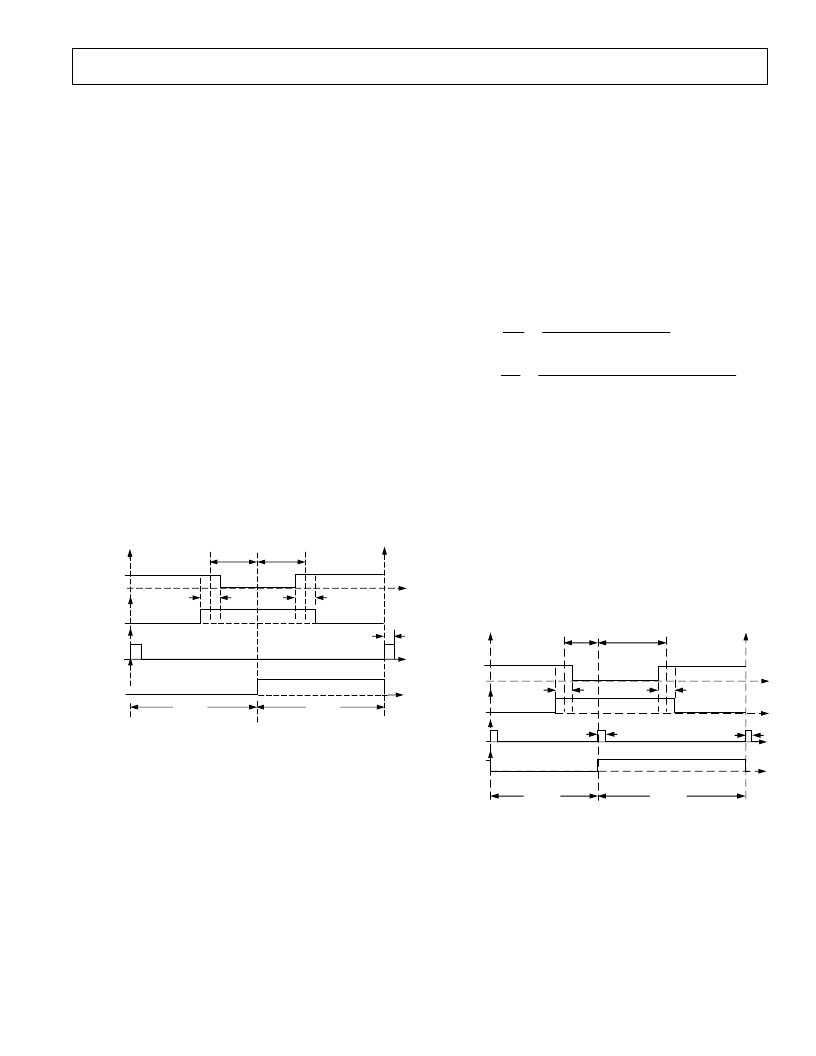
The PWM is center-based. This means that in single update mode,
the resulting output waveforms are symmetrical and centered
in the PWMSYNC period. Figure 7 presents a typical PWM timing
diagram illustrating the PWM-related registers’ (PWMCHA,
PWMTM, PWMDT, and PWMSYNCWT) control over the
waveform timing in both half cycles of the PWM period. The
magnitude of each parameter in the timing diagram is determined by
multiplying the integer value in each register by T
CK
(typically
50 ns). It may be seen in the timing diagram how dead time is
incorporated into the waveforms by moving the switching edges
away from the original values set in the PWMCHA Register.
PWMCHA
2 PWMDT
PWMSYNCWT + 1
PWMCHA
PWMTM
PWMTM
AH
AL
PWMSYNC
SYSSTAT (3)
2 PWMDT
Figure 7. Typical PWM Outputs of Three-Phase Timing
Unit in Single Update Mode
Each switching edge is moved by an equal amount (PWMDT
×
T
CK
) to preserve the symmetrical output patterns. The
PWMSYNC pulse, whose width is set by the PWMSYNCWT
Register, is also shown. Bit 3 of the SYSSTAT Register indicates
which half cycle is active. This can be useful in double update
mode, to be discussed later in this data sheet.
The resultant on-times of the PWM signals shown in Figure 5
may be written as:
T
PWMCHA
PWMDT
T
T
PWMTM
PWMCHA
PWMDT
T
AH
CK
AL
CK
=
×
×
=
×
×
2
2
(
–
)
(
–
–
)
The corresponding duty cycles are:
d
T
T
PWMCHA
PWMDT
PWMTM
d
T
T
PWMTM
PWMCHA
PWMTM
PWMDT
AH
AH
S
AL
AL
S
=
=
=
=
–
–
–
Obviously, negative values of
T
AH
and
T
AL
are not permitted
because the minimum permissible value is zero, corresponding
to a 0% duty cycle. In a similar fashion, the maximum value is
T
S
, corresponding to a 100% duty cycle.
The output signals from the timing unit for operation in double
update mode are shown in Figure 8. This illustrates a completely
general case where the switching frequency, dead time, and duty
cycle are all changed in the second half of the PWM period. Of
course, the same value for any or all of these quantities could be
used in both halves of the PWM cycle. However, it can be seen
that there is no guarantee that symmetrical PWM signals will be
produced by the timing unit in this double update mode.
Additionally, it is seen that the dead time is inserted into the PWM
signals in the same way as in the single update mode.
PWMCHA
2
2
PWMDT
1
2
PWMDT
2
PWMSYNCWT
2
+ 1
PWMCHA
1
PWMTM
1
PWMTM
2
PWMSYNCWT
1
+ 1
AH
AL
PWMSYNC
SYSSTAT (3)
Figure 8. Typical PWM Outputs of Three-Phase Timing
Unit in Double Update Mode
相關(guān)PDF資料 |
PDF描述 |
|---|---|
| ADMCF341 | DashDSP⑩ 28-Lead Flash Mixed-Signal DSP with Enhanced Analog Front End |
| ADMCF341BR | DashDSP⑩ 28-Lead Flash Mixed-Signal DSP with Enhanced Analog Front End |
| ADMCF341-EVALKIT | DashDSP⑩ 28-Lead Flash Mixed-Signal DSP with Enhanced Analog Front End |
| ADN2811 | OC-48/OC-48 FEC Clock and Data Recovery IC with Integrated Limiting Amp |
| ADN2811ACP-CML | OC-48/OC-48 FEC Clock and Data Recovery IC with Integrated Limiting Amp |
相關(guān)代理商/技術(shù)參數(shù) |
參數(shù)描述 |
|---|---|
| ADMCF340XSTB | 制造商:Analog Devices 功能描述: |
| ADMCF341 | 制造商:AD 制造商全稱:Analog Devices 功能描述:DashDSP⑩ 28-Lead Flash Mixed-Signal DSP with Enhanced Analog Front End |
| ADMCF341BR | 制造商:Analog Devices 功能描述:DSP Fixed-Point/Floating-Point 16-Bit 20MHz 20MIPS 28-Pin SOIC W T/R |
| ADMCF341BRZ-REEL | 制造商:Analog Devices 功能描述: |
| ADMCF341-EVALKIT | 制造商:AD 制造商全稱:Analog Devices 功能描述:DashDSP⑩ 28-Lead Flash Mixed-Signal DSP with Enhanced Analog Front End |
發(fā)布緊急采購(gòu),3分鐘左右您將得到回復(fù)。