- 您現(xiàn)在的位置:買賣IC網(wǎng) > PDF目錄1894 > AD9954YSVZ-REEL7 (Analog Devices Inc)IC DDS DAC 14BIT 1.8V 48TQFP PDF資料下載
參數(shù)資料
| 型號: | AD9954YSVZ-REEL7 |
| 廠商: | Analog Devices Inc |
| 文件頁數(shù): | 14/40頁 |
| 文件大?。?/td> | 0K |
| 描述: | IC DDS DAC 14BIT 1.8V 48TQFP |
| 產(chǎn)品培訓(xùn)模塊: | Direct Digital Synthesis Tutorial Series (1 of 7): Introduction Direct Digital Synthesizer Tutorial Series (7 of 7): DDS in Action Direct Digital Synthesis Tutorial Series (3 of 7): Angle to Amplitude Converter Direct Digital Synthesis Tutorial Series (6 of 7): SINC Envelope Correction Direct Digital Synthesis Tutorial Series (4 of 7): Digital-to-Analog Converter Direct Digital Synthesis Tutorial Series (2 of 7): The Accumulator |
| 標(biāo)準(zhǔn)包裝: | 500 |
| 分辨率(位): | 14 b |
| 主 fclk: | 400MHz |
| 調(diào)節(jié)字寬(位): | 32 b |
| 電源電壓: | 1.71 V ~ 1.96 V |
| 工作溫度: | -40°C ~ 105°C |
| 安裝類型: | 表面貼裝 |
| 封裝/外殼: | 48-TQFP 裸露焊盤 |
| 供應(yīng)商設(shè)備封裝: | 48-TQFP 裸露焊盤(7x7) |
| 包裝: | 帶卷 (TR) |
| 配用: | AD9954/PCBZ-ND - BOARD EVAL FOR 9954 |
第1頁第2頁第3頁第4頁第5頁第6頁第7頁第8頁第9頁第10頁第11頁第12頁第13頁當(dāng)前第14頁第15頁第16頁第17頁第18頁第19頁第20頁第21頁第22頁第23頁第24頁第25頁第26頁第27頁第28頁第29頁第30頁第31頁第32頁第33頁第34頁第35頁第36頁第37頁第38頁第39頁第40頁
AD9954
Rev. B | Page 21 of 40
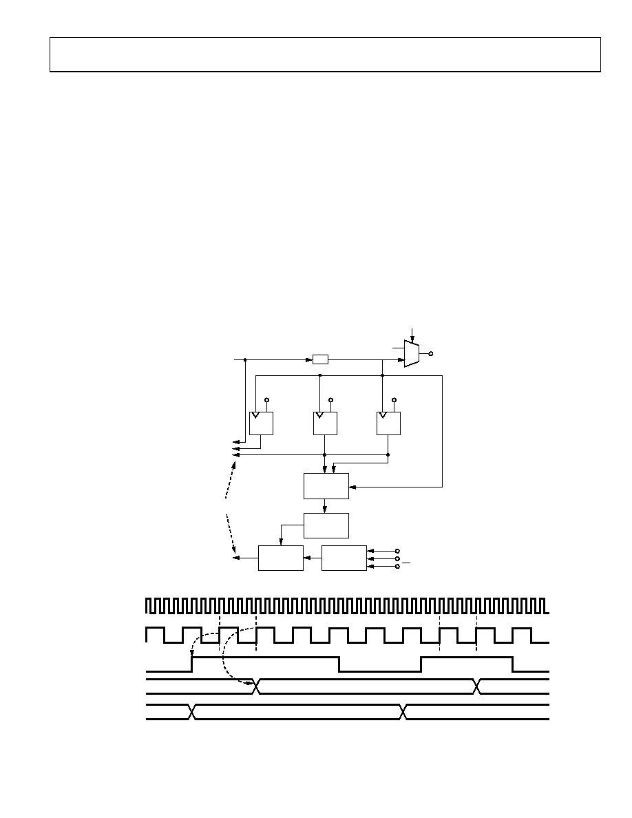
SYNCHRONIZATION—REGISTER UPDATES (I/O
UPDATE)
Functionality of the SYNC_CLK and I/O UPDATE
Data into the AD9954 is synchronous to the SYNC_CLK
signal (supplied externally to the user on the SYNC_CLK pin).
The I/O UPDATE pin is sampled on the rising edge of the
SYNC_CLK.
Internally, SYSCLK is fed to a divide-by-four frequency divider
to produce the SYNC_CLK signal. The SYNC_CLK signal is
made available to the system on the SYNC_CLK pin. This
enables synchronization of external hardware with the device’s
internal clocks. This is accomplished by providing the SYNC_CLK
signal as an output that external hardware can then use to
synchronize against.
The I/O update signal coupled with SYNC_CLK is used to
transfer internal buffer contents into the control registers. The
combination of the SYNC_CLK pin and the I/O UPDATE pin
provides the user with constant latency relative to SYSCLK and
ensures phase continuity of the analog output signal when a
new tuning word or phase offset value is asserted.
Figure 23 and Figure 24 demonstrate an I/O update timing
cycle and synchronization.
Synchronization logic notes include the following:
The I/O update signal is edge detected to generate a single-
cycle clock signal that drives the register bank flops. The I/O
update signal has no constraints on duty cycle. The minimum
low time on I/O update is one SYNC_CLK clock cycle.
The I/O UPDATE pin is set up and held around the rising
edge of SYNC_CLK. Setup and hold time specifications can
be found in Table 2.
03
37
4-
0
6
SYSCLK
SDIO
SYNC_CLK
DISABLE
10
0
SCLK
TO CORE LOGIC
CS
OSK
D
Q
PS<1:0>
D
Q
I/O UPDATE
D
Q
÷4
SYNC_CLK
GATING
EDGE
DETECTION
LOGIC
REGISTER
MEMORY
I/O BUFFER
LATCHES
Figure 23. I/O Synchronization Block Diagram
SYNC_CLK
SYSCLK
AB
DATA IN
REGISTERS
DATA IN
I/O BUFFERS
I/O UPDATE
THE DEVICE REGISTERS AN I/O UPDATE AT POINT A. THE DATA IS TRANSFERRED FROM
THE ASYNCHRONOUSLY LOADED I/O BUFFERS AT POINT B.
0
33
74
-0
07
N – 1
N
N + 1
N
N + 1
N + 2
Figure 24. I/O Synchronization Timing Diagram
相關(guān)PDF資料 |
PDF描述 |
|---|---|
| AD9956YCPZ-REEL7 | IC SYNTHESIZER 1.8V 48LFCSP |
| AD9957BSVZ-REEL | IC DDS 1GSPS 14BIT IQ 100TQFP |
| AD9958BCPZ-REEL7 | IC DDS DUAL 10BIT DAC 56LFCSP |
| AD9959BCPZ-REEL7 | IC DDS QUAD 10BIT DAC 56LFCSP |
| AD9970BCPZRL7 | IC PROCESSOR CCD SIGNAL 32-LFCSP |
相關(guān)代理商/技術(shù)參數(shù) |
參數(shù)描述 |
|---|---|
| AD9954YSVZ-REEL71 | 制造商:AD 制造商全稱:Analog Devices 功能描述:400 MSPS, 14-Bit, 1.8 V CMOS, Direct Digital Synthesizer |
| AD9955KS6 | 制造商:AD 功能描述:* |
| AD9955KS-6 | 制造商:未知廠家 制造商全稱:未知廠家 功能描述:Parallel-Input Frequency Synthesizer |
| AD9955KS-66 | 制造商:未知廠家 制造商全稱:未知廠家 功能描述:Parallel-Input Frequency Synthesizer |
| AD9956 | 制造商:AD 制造商全稱:Analog Devices 功能描述:2.7 GHz DDS-Based AgileRF |
發(fā)布緊急采購,3分鐘左右您將得到回復(fù)。