- 您現(xiàn)在的位置:買賣IC網(wǎng) > PDF目錄373970 > AD9913BCPZ-REEL71 (Analog Devices, Inc.) Low Power 250 MSPS 10-Bit DAC 1.8 V CMOS Direct Digital Synthesizer PDF資料下載
參數(shù)資料
| 型號(hào): | AD9913BCPZ-REEL71 |
| 廠商: | Analog Devices, Inc. |
| 元件分類: | XO, clock |
| 英文描述: | Low Power 250 MSPS 10-Bit DAC 1.8 V CMOS Direct Digital Synthesizer |
| 中文描述: | 低功耗250 MSPS的10位DAC 1.8伏CMOS直接數(shù)字頻率合成器 |
| 文件頁(yè)數(shù): | 18/32頁(yè) |
| 文件大小: | 473K |
| 代理商: | AD9913BCPZ-REEL71 |
第1頁(yè)第2頁(yè)第3頁(yè)第4頁(yè)第5頁(yè)第6頁(yè)第7頁(yè)第8頁(yè)第9頁(yè)第10頁(yè)第11頁(yè)第12頁(yè)第13頁(yè)第14頁(yè)第15頁(yè)第16頁(yè)第17頁(yè)當(dāng)前第18頁(yè)第19頁(yè)第20頁(yè)第21頁(yè)第22頁(yè)第23頁(yè)第24頁(yè)第25頁(yè)第26頁(yè)第27頁(yè)第28頁(yè)第29頁(yè)第30頁(yè)第31頁(yè)第32頁(yè)
AD9913
CLOCK INPUT (REF_CLK)
REF_CLK OVERVIEW
The AD9913 supports a number of options for producing the
internal SYSCLK signal (that is, the DAC sample clock) via the
REF_CLK input pins. The REF_CLK input can be driven
directly from a differential or single-ended source, or it can
accept a crystal connected across the two input pins. There is
also an internal phase-locked loop (PLL) multiplier that can be
independently enabled. The various input configurations are
controlled by means of the control bits in the CFR2 [7:5]
register.
Rev. 0 | Page 18 of 32
Table 6. Clock Input Mode Configuration
CFR2 [7:5]
Mode Configuration
000
Differential Input, PLL Enabled
001
Differential Input, PLL Disabled (Default)
x10
1
XTAL Input, PLL Enabled
x11
1
XTAL Input, PLL Disabled
100
CMOS Input, PLL Enabled
101
CMOS Input PLL Disabled
1
x = don’t care.
XTAL
REF_CLK
REF_CLK
CMOS
1
0
1
0
10
00
1
0
1
0
÷2
÷2
PLL
CFR2[5]
CFR2[6]
D
C
CFR2[5:0]
CFR2[14:9]
DIFFERENTIAL/
CFR2[15]
CFR2[3]
CFR2[7:6]
13
14
SYSTEM
0
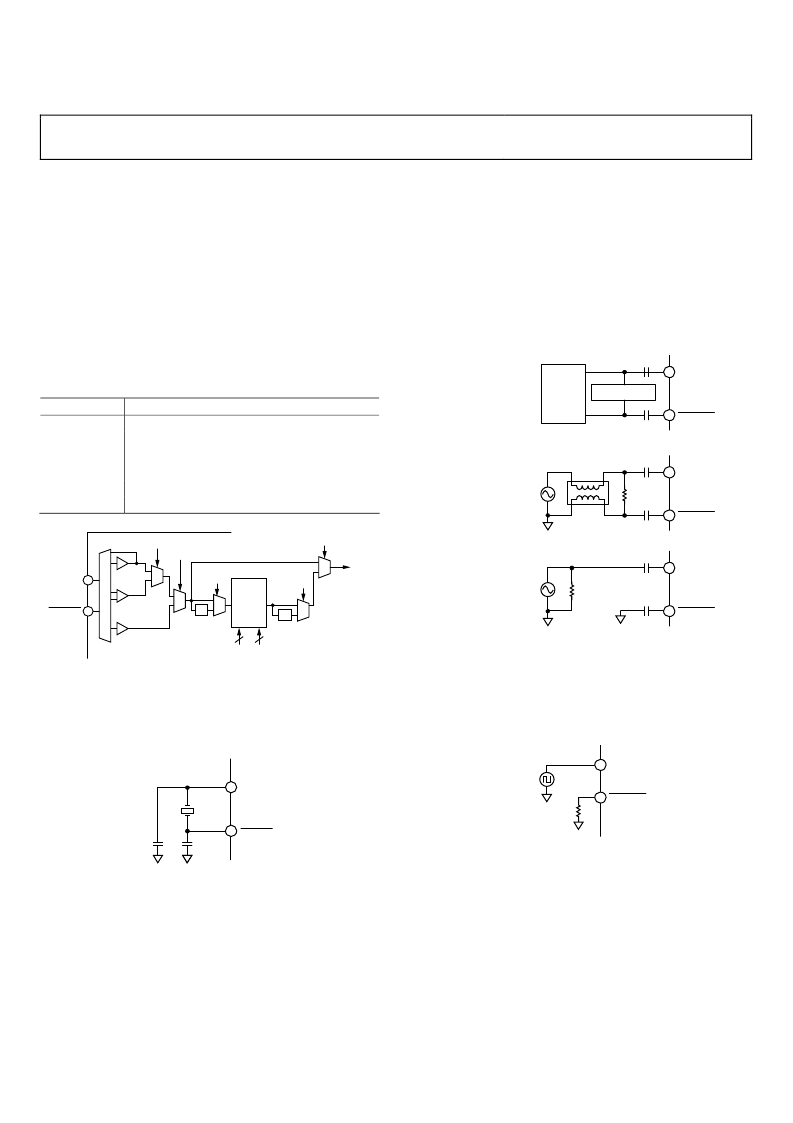
Figure 26. Internal Clock Path Functional Block Diagram
CRYSTAL-DRIVEN REF_CLK
When using a crystal at the REF_CLK input, the resonant
frequency should be approximately 25 MHz. Figure 27 shows
the recommended circuit configuration.
REFCLK
REFCLK
39pF
39pF
XTAL
13
14
0
Figure 27. Crystal Connection Diagram
DIRECT-DRIVEN REF_CLK
When driving the REF_CLK inputs directly from a signal
source, either single-ended or differential signals can be used.
With a differential signal source, the REF_CLK pins are driven
with complementary signals and ac-coupled with 0.1 μF
capacitors. With a single-ended signal source, either a single-
ended-to-differential conversion can be employed or the
REF_CLK input can be driven single-ended directly. In either
case, 0.1 μF capacitors are used to ac couple both REF_CLK
pins to avoid disturbing the internal dc bias voltage of ~1.35 V.
See Figure 28 for more details.
The REF_CLK input resistance is ~2.7 kΩ differential (~1.35 kΩ
single-ended). Most signal sources have relatively low output
impedances. The REF_CLK input resistance is relatively high,
therefore, its effect on the termination impedance is negligible
and can usually be chosen to be the same as the output imped-
ance of the signal source. The bottom two examples in Figure 28
assume a signal source with a 50 Ω output impedance.
TERMINATION
REF_CLK
DIFFERENTIAL SOURCE,
DIFFERENTIAL INPUT
SINGLE-ENDED SOURCE,
DIFFERENTIAL INPUT
SINGLE-ENDED SOURCE,
SINGLE-ENDED INPUT
13
14
0.1μF
0.1μF
LVPECL,
OR
LVDS
DRIVER
REF_CLK
13
14
50
0.1μF
0.1μF
BALUN
(1:1)
REF_CLK
REF_CLK
REF_CLK
REF_CLK
13
14
0.1μF
0.1μF
50
0
Figure 28. Direct Connection Diagram
CMOS-DRIVEN REF_CLK
This mode is enabled by writing CFR2 [7] to be true. In this
state, the AD9913 must be driven at Pin 13 with the reference
clock source. Additionally, it is recommended that Pin 14 in
CMOS mode be tied to ground through a 10 kΩ resistor.
13
14
REF_CLK
REF_CLK
10k
CMOS
DRIVER
0
Figure 29. CMOS-Driven Diagram
PHASE-LOCKED LOOP (PLL) MULTIPLIER
An internal phase-locked loop (PLL) provides users of the
AD9913 the option to use a reference clock frequency that is
lower than the system clock frequency. The PLL supports a wide
range of programmable frequency multiplication factors (1× to
64×). See
Table 7
for details on configuring the PLL multipli-
cation factor. The PLL is also equipped with a PLL_LOCK bit.
CFR2 [15:8] and CFR2 [5:1] control the PLL operation. Upon
power-up, the PLL is off. To initialize the PLL, CFR2 [5] must
be cleared and CFR2 [1] must be set. The function of CFR2 [1]
相關(guān)PDF資料 |
PDF描述 |
|---|---|
| AD9920A | 12-Bit CCD Signal Processor with V-Driver and Precision Timing Generator |
| AD9923A | CCD Signal Processor with V-Driver and Precision Timing⑩ Generator |
| AD9923ABBCZ | CCD Signal Processor with V-Driver and Precision Timing⑩ Generator |
| AD9923ABBCZRL | CCD Signal Processor with V-Driver and Precision Timing⑩ Generator |
| AD9925BBCZRL | CCD Signal Processor with Vertical Driver and Precision Timing Generator |
相關(guān)代理商/技術(shù)參數(shù) |
參數(shù)描述 |
|---|---|
| AD9914 | 制造商:AD 制造商全稱:Analog Devices 功能描述:3.5 GSPS Direct Digital Synthesizer with 12-Bit DAC |
| AD9914/PCBZ | 功能描述:數(shù)據(jù)轉(zhuǎn)換 IC 開(kāi)發(fā)工具 3.5 GSPS DDS w/Upconverter eval bd. RoHS:否 制造商:Texas Instruments 產(chǎn)品:Demonstration Kits 類型:ADC 工具用于評(píng)估:ADS130E08 接口類型:SPI 工作電源電壓:- 6 V to + 6 V |
| AD9914BCPZ | 功能描述:數(shù)據(jù)轉(zhuǎn)換 IC - 多種 3.5 GSPS DDS w/Upconverter RoHS:否 制造商:Texas Instruments 轉(zhuǎn)換器數(shù)量:1 分辨率:8 bit 工作電源電壓:2.7 V to 5.5 V 功耗: 工作溫度范圍:- 40 C to + 85 C 封裝 / 箱體:MSOP-10 封裝:Reel |
| AD9914BCPZ-REEL7 | 功能描述:數(shù)據(jù)轉(zhuǎn)換 IC - 多種 3.5 GSPS DDS w/Upconverter RoHS:否 制造商:Texas Instruments 轉(zhuǎn)換器數(shù)量:1 分辨率:8 bit 工作電源電壓:2.7 V to 5.5 V 功耗: 工作溫度范圍:- 40 C to + 85 C 封裝 / 箱體:MSOP-10 封裝:Reel |
| AD9914PCBZ | 制造商:AD 制造商全稱:Analog Devices 功能描述:3.5 GSPS Direct Digital Synthesizer with 12-Bit DAC |
發(fā)布緊急采購(gòu),3分鐘左右您將得到回復(fù)。