- 您現(xiàn)在的位置:買賣IC網(wǎng) > PDF目錄2062 > AD8317ACPZ-R7 (Analog Devices Inc)IC AMP LOG DETECT 8GHZ 8-LFCSP PDF資料下載
參數(shù)資料
| 型號: | AD8317ACPZ-R7 |
| 廠商: | Analog Devices Inc |
| 文件頁數(shù): | 5/20頁 |
| 文件大?。?/td> | 0K |
| 描述: | IC AMP LOG DETECT 8GHZ 8-LFCSP |
| 產(chǎn)品培訓模塊: | Choosing and Using RF Detectors |
| 標準包裝: | 1 |
| 類型: | 對數(shù)放大器 |
| 應用: | 接收器信號強度指示(RSSI) |
| 安裝類型: | 表面貼裝 |
| 封裝/外殼: | 8-VFDFN 裸露焊盤 |
| 供應商設(shè)備封裝: | 8-LFCSP-VD(3x2) |
| 包裝: | 標準包裝 |
| 產(chǎn)品目錄頁面: | 550 (CN2011-ZH PDF) |
| 其它名稱: | AD8317ACPZ-R7DKR |
AD8317
Rev. B | Page 13 of 20
For example, PINTERCEPT for a sinusoidal input signal expressed in
terms of dBm (decibels referred to 1 mW), in a 50 Ω system is
PINTERCEPT [dBm] =
PINTERCEPT [dBV] 10 × log10(Z0 × 1 mW/1 VRMS2) =
2 dBV 10 × log10(50 × 103) = 15 dBm
(8)
For a square wave input signal in a 200 Ω system,
PINTERCEPT =
1 dBV 10 × log10[(200 Ω × 1 mW/1 VRMS2)] = 6 dBm
Further information on the intercept variation dependence
data sheets.
SETTING THE OUTPUT SLOPE IN MEASUREMENT
MODE
To operate in measurement mode, VOUT must be connected
to VSET. Connecting VOUT directly to VSET yields the nominal
logarithmic slope of approximately 22 mV/dB. The output
swing corresponding to the specified input range is then approx-
imately 0.35 V to 1.7 V. The slope and output swing can be
increased by placing a resistor divider between VOUT and
VSET (that is, one resistor from VOUT to VSET and one
resistor from VSET to ground). The input impedance of VSET
is approximately 40 kΩ. Slope-setting resistors should be kept
below 20 kΩ to prevent this input impedance from affecting
the resulting slope. If two equal resistors are used (for example,
10 kΩ/10 kΩ), the slope doubles to approximately 44 mV/dB.
05
54
1-
0
28
VOUT
AD8317
–44mV/dB
VSET
10k
Figure 28. Increasing the Slope
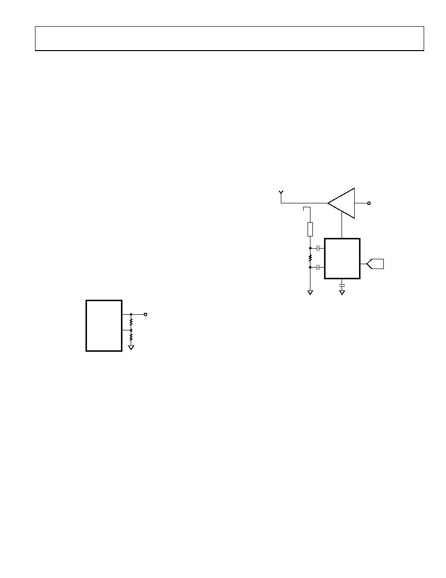
CONTROLLER MODE
The AD8317 provides a controller mode feature at the VOUT
pin. By using VSET for the setpoint voltage, it is possible for the
AD8317 to control subsystems, such as power amplifiers (PAs),
variable gain amplifiers (VGAs), or variable voltage attenuators
(VVAs), that have output power that increases monotonically
with respect to their gain control signal.
To operate in controller mode, the link between VSET and
VOUT is broken. A setpoint voltage is applied to the VSET
input, VOUT is connected to the gain control terminal of the
VGA, and the RF input of the detector is connected to the
output of the VGA (usually using a directional coupler and
some additional attenuation). Based on the defined relationship
between VOUT and the RF input signal when the device is in
measurement mode, the AD8317 adjusts the voltage on VOUT
(VOUT is now an error amplifier output) until the level at the
RF input corresponds to the applied VSET. When the AD8317
operates in controller mode, there is no defined relationship
between the VSET and the VOUT voltage; VOUT settles to a value
that results in the correct input signal level appearing at
INHI/INLO.
For this output power control loop to be stable, a ground-
referenced capacitor must be connected to the CLPF pin. This
capacitor, CFLT, integrates the error signal (in the form of a
current) to set the loop bandwidth and ensure loop stability.
Further details on control loop dynamics can be found in the
AD8315 data sheet.
05
54
1-
0
29
RFIN
VGA/VVA
GAIN
CONTROL
VOLTAGE
DIRECTIONAL
COUPLER
ATTENUATOR
INHI
VSET
INLO
CLPF
VOUT
AD8317
52.3
47nF
CFLT
47nF
DAC
Figure 29. Controller Mode
Decreasing VSET, which corresponds to demanding a higher
signal from the VGA, increases VOUT. The gain control voltage
of the VGA must have a positive sense. A positive control
voltage to the VGA increases the gain of the device.
The basic connections for operating the AD8317 in an auto-
matic gain control (AGC) loop with the ADL5330 are shown in
Figure 30. The ADL5330 is a 10 MHz to 3 GHz VGA. It offers a
large gain control range of 60 dB with ±0.5 dB gain stability.
This configuration is similar to Figure 29.
The gain of the ADL5330 is controlled by the output pin of the
AD8317. This voltage, VOUT, has a range of 0 V to near VPOS. To
avoid overdrive recovery issues, the AD8317 output voltage can
be scaled down using a resistive divider to interface with the 0 V
to 1.4 V gain control range of the ADL5330.
A coupler/attenuation of 21 dB is used to match the desired
maximum output power from the VGA to the top end of the
linear operating range of the AD8317 (approximately 5 dBm
at 900 MHz).
相關(guān)PDF資料 |
PDF描述 |
|---|---|
| AD8321ARZ | IC LINE DRIVER CATV 3.3V 20SOIC |
| AD8322ARUZ-REEL | IC LN DVR CATV COARS-STP 28TSSOP |
| AD8324JRQZ-REEL | IC LINE DRIVER CBL 3.3V 20QSOP |
| AD8325ARUZ-REEL | IC LN DVR CATV FINE-STEP 28TSSOP |
| AD8326AREZ | IC LINE DVR CATV PROG 28TSSOP |
相關(guān)代理商/技術(shù)參數(shù) |
參數(shù)描述 |
|---|---|
| AD8317ACPZ-R7 | 制造商:Analog Devices 功能描述:IC LOGARITHMIC AMPLIFIER 20NS LFCSP-8 |
| AD8317ACPZ-WP | 制造商:Analog Devices 功能描述: |
| AD8317-EVAL | 制造商:AD 制造商全稱:Analog Devices 功能描述:1 MHz to 10 GHz, 50 dB Log Detector/Controller |
| AD8317-EVALZ | 制造商:Analog Devices 功能描述:EVAL KIT FOR 1 MHZ TO 10 GHZ, 50 DB LOG DETECTOR/CNTRLR - Bulk 制造商:Analog Devices 功能描述:EVAL BOARD, AD8317 LOG DETECTOR/CNTRL, Silicon Manufacturer:Analog Devices, Silicon Core Number:AD8317, Kit Application Type:RF / IF, Kit Contents:Eval Board AD8317, Features:(Not Applicable) |
| AD8318 | 制造商:AD 制造商全稱:Analog Devices 功能描述:1 MHz to 8 GHz, 70 dB Logarithmic Detector/Controller |
發(fā)布緊急采購,3分鐘左右您將得到回復。