- 您現(xiàn)在的位置:買賣IC網(wǎng) > PDF目錄2062 > AD8317ACPZ-R7 (Analog Devices Inc)IC AMP LOG DETECT 8GHZ 8-LFCSP PDF資料下載
參數(shù)資料
| 型號(hào): | AD8317ACPZ-R7 |
| 廠商: | Analog Devices Inc |
| 文件頁數(shù): | 4/20頁 |
| 文件大小: | 0K |
| 描述: | IC AMP LOG DETECT 8GHZ 8-LFCSP |
| 產(chǎn)品培訓(xùn)模塊: | Choosing and Using RF Detectors |
| 標(biāo)準(zhǔn)包裝: | 1 |
| 類型: | 對(duì)數(shù)放大器 |
| 應(yīng)用: | 接收器信號(hào)強(qiáng)度指示(RSSI) |
| 安裝類型: | 表面貼裝 |
| 封裝/外殼: | 8-VFDFN 裸露焊盤 |
| 供應(yīng)商設(shè)備封裝: | 8-LFCSP-VD(3x2) |
| 包裝: | 標(biāo)準(zhǔn)包裝 |
| 產(chǎn)品目錄頁面: | 550 (CN2011-ZH PDF) |
| 其它名稱: | AD8317ACPZ-R7DKR |
AD8317
Rev. B | Page 12 of 20
The slope is given by
ID × 2x × 1.5 kΩ = 22 mV/dB × x
For example, if a resistor divider to ground is used to generate a
VSET voltage of VOUT/2, x = 2. The slope is set to 880 V/decade
or 44 mV/dB.
TEMPERATURE COMPENSATION OF OUTPUT
VOLTAGE
The primary component of the variation in VOUT vs. temperature,
as the input signal amplitude is held constant, is the drift of the
intercept. This drift is also a weak function of the input signal
frequency; therefore, provision is made for the optimization of
internal temperature compensation at a given frequency by
providing Pin TADJ.
COMM
ICOMP
VINTERNAL
TADJ
RTADJ
05
54
1-
02
6
1.5k
AD8317
Figure 26. TADJ Interface
RTADJ is connected between TADJ and ground. The value of
this resistor partially determines the magnitude of an analog
correction coefficient, which is used to reduce intercept drift.
The relationship between output temperature drift and
frequency is not linear and cannot be easily modeled. As a
result, experimentation is required to choose the correct
TADJ resistor. Table 4 shows the recommended values for
some commonly used frequencies.
Table 4. Recommended RTADJ Values
Frequency
Recommended RTADJ
50 MHz
18 kΩ
100 MHz
18 kΩ
900 MHz
18 kΩ
1.8 GHz
8 kΩ
1.9 GHz
8 kΩ
2.2 GHz
8 kΩ
3.6 GHz
8 kΩ
5.3 GHZ
500 Ω
5.8 GHz
500 Ω
8 GHz
Open
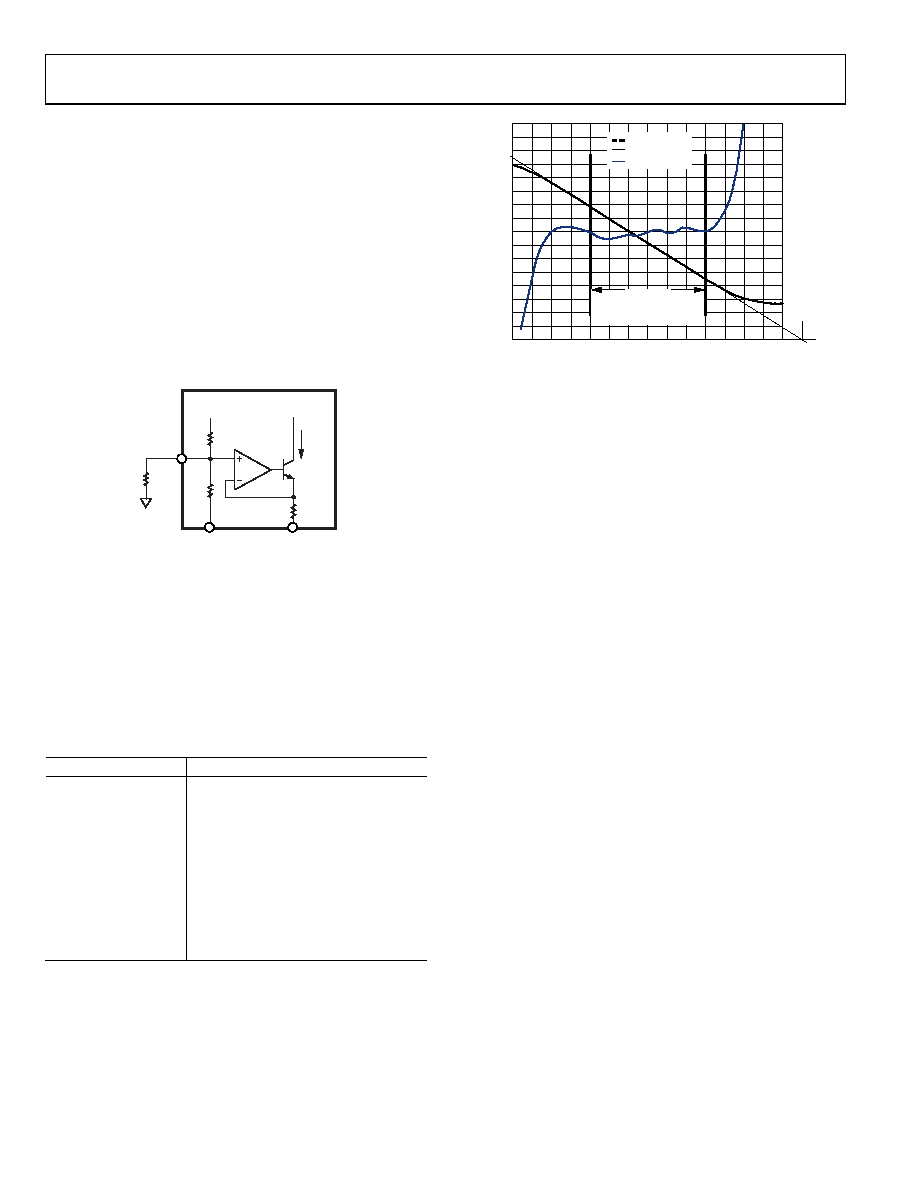
MEASUREMENT MODE
When the VOUT voltage or a portion of the VOUT voltage is fed
back to the VSET pin, the device operates in measurement
mode. As seen in Figure 27, the AD8317 has an offset voltage,
a negative slope, and a VOUT measurement intercept at the high
end of its input signal range.
0
0.25
0.50
0.75
1.00
1.25
1.50
2.00
V
OU
T
(V
)
–1.5
–1.0
–0.5
0
0.5
1.0
1.5
2.0
–60 –55 –50 –45 –40 –35 –30 –25 –20 –15 –10 –5
0
5
10 15
PIN (dBm)
05
54
1-
02
7
RANGE FOR
CALCULATION OF
SLOPE AND INTERCEPT
VOUT IDEAL
VOUT 25°C
ERROR 25°C
1.75
INTERCEPT
Figure 27. Typical Output Voltage vs. Input Signal
The output voltage vs. input signal voltage of the AD8317 is
linear-in-dB over a multidecade range. The equation for this
function is
VOUT = X × VSLOPE/DEC × log10(VIN/VINTERCEPT)
(3)
= X × VSLOPE/dB × 20 × log10(VIN/VINTERCEPT)
(4)
where:
X is the feedback factor in VSET = VOUT/X.
VSLOPE/DEC is nominally 440 mV/decade, or 22 mV/dB.
VINTERCEPT is the x-axis intercept of the linear-in-dB portion of
VINTERCEPT is 2 dBV for a sinusoidal input signal.
An offset voltage, VOFFSET, of 0.35 V is internally added to
the detector signal, so that the minimum value for VOUT is
X × VOFFSET; therefore, for X = 1, the minimum VOUT is 0.35 V.
The slope is very stable vs. process and temperature variation.
When base-10 logarithms are used, VSLOPE/DECADE represents the
volts/decade. A decade corresponds to 20 dB; VSLOPE/DECADE/20 =
VSLOPE/dB represents the slope in volts/dB.
negative slope. This is also the correct slope polarity to control
the gain of many power amplifiers in a negative feedback con-
figuration. Because both the slope and intercept vary slightly
with frequency, it is recommended to refer to the Specifications
section for application-specific values for slope and intercept.
Although demodulating log amps respond to input signal
voltage, not input signal power, it is customary to discuss the
amplitude of high frequency signals in terms of power. In this
case, the characteristic impedance of the system, Z0, must be
known to convert voltages to their corresponding power levels.
The following equations are used to perform this conversion:
P [dBm] = 10 × log10(VRMS2/(Z0 × 1 mW))
(5)
P [dBV] = 20 × log10(VRMS/1 VRMS)
(6)
P [dBm] = P [dBV] 10 × log10(Z0 × 1 mW/1 VRMS2)
(7)
相關(guān)PDF資料 |
PDF描述 |
|---|---|
| AD8321ARZ | IC LINE DRIVER CATV 3.3V 20SOIC |
| AD8322ARUZ-REEL | IC LN DVR CATV COARS-STP 28TSSOP |
| AD8324JRQZ-REEL | IC LINE DRIVER CBL 3.3V 20QSOP |
| AD8325ARUZ-REEL | IC LN DVR CATV FINE-STEP 28TSSOP |
| AD8326AREZ | IC LINE DVR CATV PROG 28TSSOP |
相關(guān)代理商/技術(shù)參數(shù) |
參數(shù)描述 |
|---|---|
| AD8317ACPZ-R7 | 制造商:Analog Devices 功能描述:IC LOGARITHMIC AMPLIFIER 20NS LFCSP-8 |
| AD8317ACPZ-WP | 制造商:Analog Devices 功能描述: |
| AD8317-EVAL | 制造商:AD 制造商全稱:Analog Devices 功能描述:1 MHz to 10 GHz, 50 dB Log Detector/Controller |
| AD8317-EVALZ | 制造商:Analog Devices 功能描述:EVAL KIT FOR 1 MHZ TO 10 GHZ, 50 DB LOG DETECTOR/CNTRLR - Bulk 制造商:Analog Devices 功能描述:EVAL BOARD, AD8317 LOG DETECTOR/CNTRL, Silicon Manufacturer:Analog Devices, Silicon Core Number:AD8317, Kit Application Type:RF / IF, Kit Contents:Eval Board AD8317, Features:(Not Applicable) |
| AD8318 | 制造商:AD 制造商全稱:Analog Devices 功能描述:1 MHz to 8 GHz, 70 dB Logarithmic Detector/Controller |
發(fā)布緊急采購,3分鐘左右您將得到回復(fù)。