- 您現(xiàn)在的位置:買賣IC網(wǎng) > PDF目錄36339 > 935267395551 (NXP SEMICONDUCTORS) COLOR SIGNAL DECODER, PBGA156 PDF資料下載
參數(shù)資料
| 型號: | 935267395551 |
| 廠商: | NXP SEMICONDUCTORS |
| 元件分類: | 顏色信號轉換 |
| 英文描述: | COLOR SIGNAL DECODER, PBGA156 |
| 封裝: | 15 X 15 MM, 1.15 MM HEIGHT, PLASTIC, MS-034, SOT-472-1, BGA-156 |
| 文件頁數(shù): | 176/178頁 |
| 文件大小: | 988K |
| 代理商: | 935267395551 |
第1頁第2頁第3頁第4頁第5頁第6頁第7頁第8頁第9頁第10頁第11頁第12頁第13頁第14頁第15頁第16頁第17頁第18頁第19頁第20頁第21頁第22頁第23頁第24頁第25頁第26頁第27頁第28頁第29頁第30頁第31頁第32頁第33頁第34頁第35頁第36頁第37頁第38頁第39頁第40頁第41頁第42頁第43頁第44頁第45頁第46頁第47頁第48頁第49頁第50頁第51頁第52頁第53頁第54頁第55頁第56頁第57頁第58頁第59頁第60頁第61頁第62頁第63頁第64頁第65頁第66頁第67頁第68頁第69頁第70頁第71頁第72頁第73頁第74頁第75頁第76頁第77頁第78頁第79頁第80頁第81頁第82頁第83頁第84頁第85頁第86頁第87頁第88頁第89頁第90頁第91頁第92頁第93頁第94頁第95頁第96頁第97頁第98頁第99頁第100頁第101頁第102頁第103頁第104頁第105頁第106頁第107頁第108頁第109頁第110頁第111頁第112頁第113頁第114頁第115頁第116頁第117頁第118頁第119頁第120頁第121頁第122頁第123頁第124頁第125頁第126頁第127頁第128頁第129頁第130頁第131頁第132頁第133頁第134頁第135頁第136頁第137頁第138頁第139頁第140頁第141頁第142頁第143頁第144頁第145頁第146頁第147頁第148頁第149頁第150頁第151頁第152頁第153頁第154頁第155頁第156頁第157頁第158頁第159頁第160頁第161頁第162頁第163頁第164頁第165頁第166頁第167頁第168頁第169頁第170頁第171頁第172頁第173頁第174頁第175頁當前第176頁第177頁第178頁
2004
Jul
22
97
Philips
Semiconductors
Product
speci
cation
Multistandard
video
decoder
with
adaptiv
e
comb
lter
and
component
video
input
SAA7118
2004
Jul
22
97
Philips
Semiconductors
Product
speci
cation
Multistandard
video
decoder
with
adaptiv
e
comb
lter
and
component
video
input
SAA7118
This text is here in white to force landscape pages to be rotated correctly when browsing through the pdf in the Acrobat reader.This text is here in
_white to force landscape pages to be rotated correctly when browsing through the pdf in the Acrobat reader.This text is here inThis text is here in
white to force landscape pages to be rotated correctly when browsing through the pdf in the Acrobat reader. white to force landscape pages to be ...
Reserved
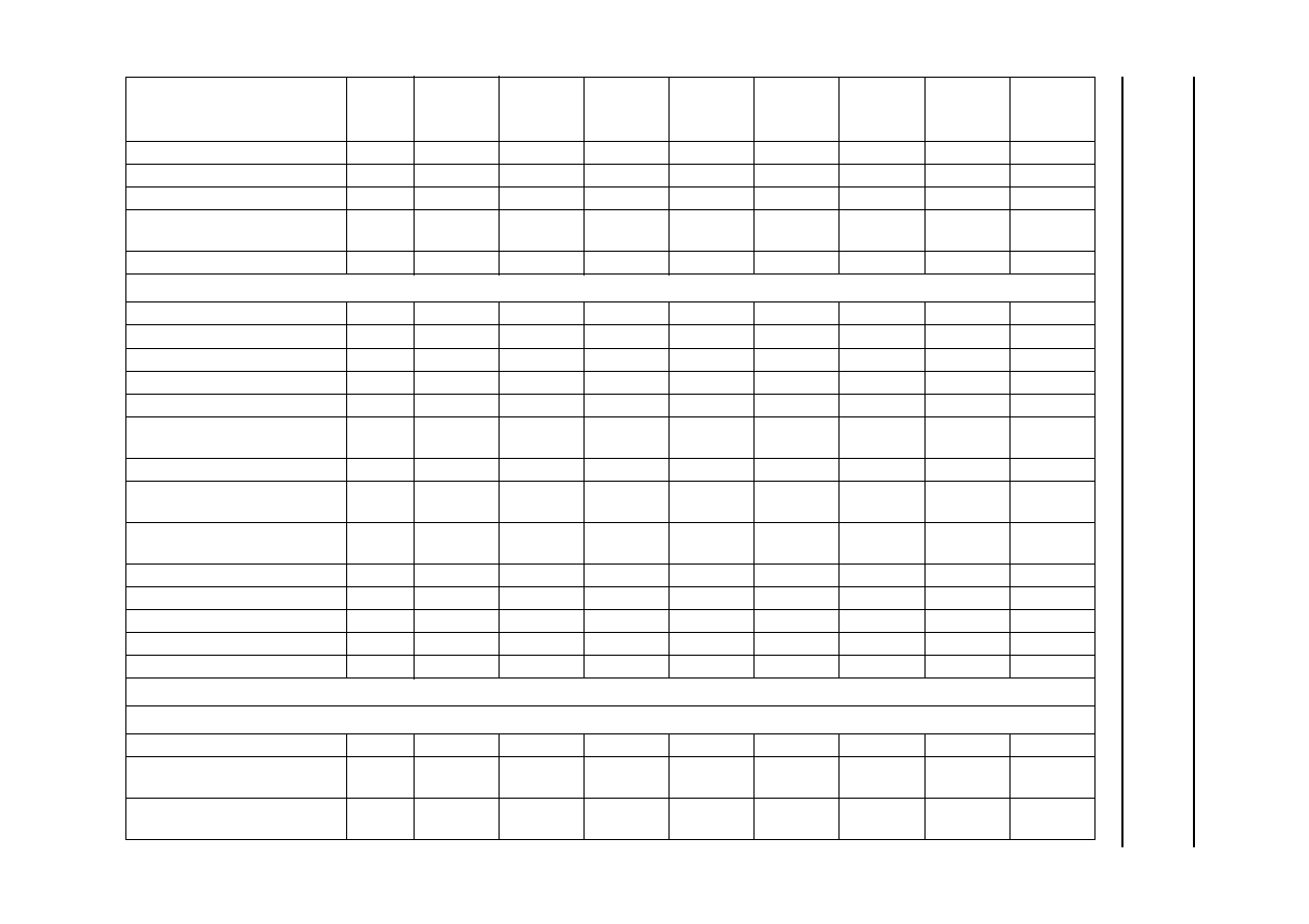
37
Clock ratio AMXCLK to ASCLK
38
SDIV5
SDIV4
SDIV3
SDIV2
SDIV1
SDIV0
Clock ratio ASCLK to ALRCLK
39
LRDIV5
LRDIV4
LRDIV3
LRDIV2
LRDIV1
LRDIV0
Audio clock generator basic
setup
3A
APLL
AMVR
LRPH
SCPH
Reserved
3B to 3F
General purpose VBI data slicer part: registers 40H to 7FH
Slicer control 1
40
HAM_N
FCE
HUNT_N
LCR2 to LCR24 (n = 2 to 24)
41 to 57
LCRn_7
LCRn_6
LCRn_5
LCRn_4
LCRn_3
LCRn_2
LCRn_1
LCRn_0
Programmable framing code
58
FC7
FC6
FC5
FC4
FC3
FC2
FC1
FC0
Horizontal offset for slicer
59
HOFF7
HOFF6
HOFF5
HOFF4
HOFF3
HOFF2
HOFF1
HOFF0
Vertical offset for slicer
5A
VOFF7
VOFF6
VOFF5
VOFF4
VOFF3
VOFF2
VOFF1
VOFF0
Field offset and MSBs for
horizontal and vertical offset
5B
FOFF
RECODE
VOFF8
HOFF10
HOFF9
HOFF8
Reserved (for testing)
5C
Header and data identication
(DID) code control
5D
FVREF
DID5
DID4
DID3
DID2
DID1
DID0
Sliced data identication (SDID)
code
5E
SDID5
SDID4
SDID3
SDID2
SDID1
SDID0
Reserved
5F
Slicer status byte 0 (read only)
60
FC8V
FC7V
VPSV
PPV
CCV
Slicer status byte 1 (read only)
61
F21_N
LN8
LN7
LN6
LN5
LN4
Slicer status byte 2 (read only)
62
LN3
LN2
LN1
LN0
DT3
DT2
DT1
DT0
Reserved
63 to 7F
X port, I port and the scaler part: registers 80H to EFH
TASK INDEPENDENT GLOBAL SETTINGS: 80H TO 8FH
Global control 1
80
SMOD
TEB
TEA
ICKS3
ICKS2
ICKS1
ICKS0
Reserved
81 and
82
X port I/O enable and output
clock phase control
83
XPCK1
XPCK0
XRQT
XPE1
XPE0
REGISTER FUNCTION
SUB
ADDR.
(HEX)
D7
D6
D5
D4
D3
D2
D1
D0
相關PDF資料 |
PDF描述 |
|---|---|
| 935267395557 | COLOR SIGNAL DECODER, PBGA156 |
| 935268832557 | COLOR SIGNAL DECODER, PQFP160 |
| 935273916518 | COLOR SIGNAL DECODER, PBGA156 |
| 935273916557 | COLOR SIGNAL DECODER, PBGA156 |
| 935268460118 | 1-CHANNEL, SGL POLE SGL THROW SWITCH, PDSO5 |
相關代理商/技術參數(shù) |
參數(shù)描述 |
|---|---|
| 935268081112 | 制造商:NXP Semiconductors 功能描述:SUB ONLY IC |
| 935268721125 | 制造商:NXP Semiconductors 功能描述:Buffer/Line Driver 1-CH Non-Inverting 3-ST CMOS 5-Pin TSSOP T/R |
| 935269304128 | 制造商:ST-Ericsson 功能描述:IC AUDIO CODEC W/TCH SCRN 48LQFP |
| 935269544557 | 制造商:NXP Semiconductors 功能描述:SUB ONLY TDA9587-2US1-V1.3 |
| 935269987557 | 制造商:NXP Semiconductors 功能描述:SUB ONLY TDA9587-1US1-V1.8 SUBBED TO 935269987557 |
發(fā)布緊急采購,3分鐘左右您將得到回復。