- 您現(xiàn)在的位置:買(mǎi)賣(mài)IC網(wǎng) > PDF目錄36339 > 935267395551 (NXP SEMICONDUCTORS) COLOR SIGNAL DECODER, PBGA156 PDF資料下載
參數(shù)資料
| 型號(hào): | 935267395551 |
| 廠商: | NXP SEMICONDUCTORS |
| 元件分類: | 顏色信號(hào)轉(zhuǎn)換 |
| 英文描述: | COLOR SIGNAL DECODER, PBGA156 |
| 封裝: | 15 X 15 MM, 1.15 MM HEIGHT, PLASTIC, MS-034, SOT-472-1, BGA-156 |
| 文件頁(yè)數(shù): | 168/178頁(yè) |
| 文件大小: | 988K |
| 代理商: | 935267395551 |
第1頁(yè)第2頁(yè)第3頁(yè)第4頁(yè)第5頁(yè)第6頁(yè)第7頁(yè)第8頁(yè)第9頁(yè)第10頁(yè)第11頁(yè)第12頁(yè)第13頁(yè)第14頁(yè)第15頁(yè)第16頁(yè)第17頁(yè)第18頁(yè)第19頁(yè)第20頁(yè)第21頁(yè)第22頁(yè)第23頁(yè)第24頁(yè)第25頁(yè)第26頁(yè)第27頁(yè)第28頁(yè)第29頁(yè)第30頁(yè)第31頁(yè)第32頁(yè)第33頁(yè)第34頁(yè)第35頁(yè)第36頁(yè)第37頁(yè)第38頁(yè)第39頁(yè)第40頁(yè)第41頁(yè)第42頁(yè)第43頁(yè)第44頁(yè)第45頁(yè)第46頁(yè)第47頁(yè)第48頁(yè)第49頁(yè)第50頁(yè)第51頁(yè)第52頁(yè)第53頁(yè)第54頁(yè)第55頁(yè)第56頁(yè)第57頁(yè)第58頁(yè)第59頁(yè)第60頁(yè)第61頁(yè)第62頁(yè)第63頁(yè)第64頁(yè)第65頁(yè)第66頁(yè)第67頁(yè)第68頁(yè)第69頁(yè)第70頁(yè)第71頁(yè)第72頁(yè)第73頁(yè)第74頁(yè)第75頁(yè)第76頁(yè)第77頁(yè)第78頁(yè)第79頁(yè)第80頁(yè)第81頁(yè)第82頁(yè)第83頁(yè)第84頁(yè)第85頁(yè)第86頁(yè)第87頁(yè)第88頁(yè)第89頁(yè)第90頁(yè)第91頁(yè)第92頁(yè)第93頁(yè)第94頁(yè)第95頁(yè)第96頁(yè)第97頁(yè)第98頁(yè)第99頁(yè)第100頁(yè)第101頁(yè)第102頁(yè)第103頁(yè)第104頁(yè)第105頁(yè)第106頁(yè)第107頁(yè)第108頁(yè)第109頁(yè)第110頁(yè)第111頁(yè)第112頁(yè)第113頁(yè)第114頁(yè)第115頁(yè)第116頁(yè)第117頁(yè)第118頁(yè)第119頁(yè)第120頁(yè)第121頁(yè)第122頁(yè)第123頁(yè)第124頁(yè)第125頁(yè)第126頁(yè)第127頁(yè)第128頁(yè)第129頁(yè)第130頁(yè)第131頁(yè)第132頁(yè)第133頁(yè)第134頁(yè)第135頁(yè)第136頁(yè)第137頁(yè)第138頁(yè)第139頁(yè)第140頁(yè)第141頁(yè)第142頁(yè)第143頁(yè)第144頁(yè)第145頁(yè)第146頁(yè)第147頁(yè)第148頁(yè)第149頁(yè)第150頁(yè)第151頁(yè)第152頁(yè)第153頁(yè)第154頁(yè)第155頁(yè)第156頁(yè)第157頁(yè)第158頁(yè)第159頁(yè)第160頁(yè)第161頁(yè)第162頁(yè)第163頁(yè)第164頁(yè)第165頁(yè)第166頁(yè)第167頁(yè)當(dāng)前第168頁(yè)第169頁(yè)第170頁(yè)第171頁(yè)第172頁(yè)第173頁(yè)第174頁(yè)第175頁(yè)第176頁(yè)第177頁(yè)第178頁(yè)
2004 Jul 22
9
Philips Semiconductors
Product specication
Multistandard video decoder with adaptive
comb lter and component video input
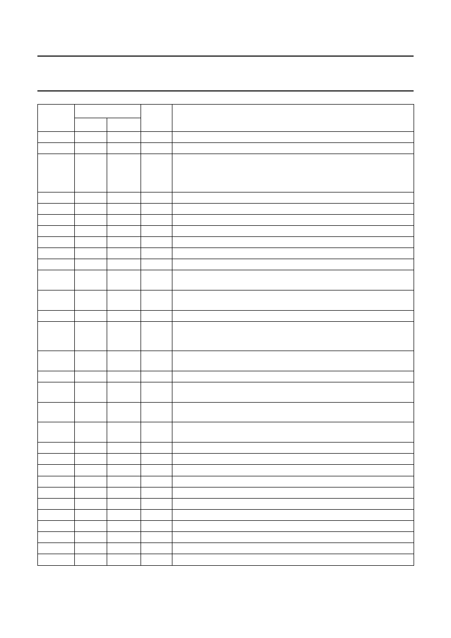
SAA7118
VDDD5
73
M11
P
digital supply voltage 5 (peripheral cells)
ASCLK
74
N11
O
audio serial clock output
ALRCLK
75
P12
O/st/pd
audio left/right clock output; can be strapped to supply via a 3.3 k
resistor
to indicate that the default 24.576 MHz crystal (ALRCLK = 0; internal
pull-down) has been replaced by a 32.110 MHz crystal (ALRCLK = 1);
AMXCLK
76
M12
I
audio master external clock input
ITRDY
77
N12
I/pu
target ready input for image port data
DNC0
78
P13
I/pu
do not connect, reserved for future extensions and for testing: scan input
DNC16
79
N13
NC
do not connect, reserved for future extensions and for testing
DNC17
80
N14
NC
do not connect, reserved for future extensions and for testing
DNC19
81
NC
do not connect, reserved for future extensions and for testing
DNC20
82
NC
do not connect, reserved for future extensions and for testing
FSW
83
M13
I/pd
fast switch (blanking) with internal pull-down inserts component inputs into
CVBS signal
ICLK
84
M14
I/O
clock output signal for image port, or optional asynchronous back-end
clock input
IDQ
85
L13
O
output data qualier for image port (optional: gated clock output)
ITRI
86
L12
I/(O)
image port output control signal, affects all input port pins inclusive ICLK,
enable and active polarity is under software control (bits IPE in subaddress
87H); output path used for testing: scan output
IGP0
87
L14
O
general purpose output signal 0; image port (controlled by subaddresses
84H and 85H)
VSSD5
88
L11
P
digital ground 5 (peripheral cells)
IGP1
89
K13
O
general purpose output signal 1; image port (controlled by subaddresses
84H and 85H)
IGPV
90
K14
O
multi purpose vertical reference output signal; image port (controlled by
subaddresses 84H and 85H)
IGPH
91
K12
O
multi purpose horizontal reference output signal; image port (controlled by
subaddresses 84H and 85H)
IPD7
92
K11
O
MSB of image port data output
IPD6
93
J13
O
MSB
1 of image port data output
IPD5
94
J14
O
MSB
2 of image port data output
VDDD6
95
J12
P
digital supply voltage 6 (core)
VSSD6
96
J11
P
digital ground 6 (core)
IPD4
97
H13
O
MSB
3 of image port data output
IPD3
98
H14
O
MSB
4 of image port data output
IPD2
99
H11
O
MSB
5 of image port data output
IPD1
100
G12
O
MSB
6 of image port data output
VDDD7
101
H12
P
digital supply voltage 7 (peripheral cells)
IPD0
102
G14
O
LSB of image port data output
SYMBOL
PIN
TYPE(1)
DESCRIPTION
QFP160 BGA156
相關(guān)PDF資料 |
PDF描述 |
|---|---|
| 935267395557 | COLOR SIGNAL DECODER, PBGA156 |
| 935268832557 | COLOR SIGNAL DECODER, PQFP160 |
| 935273916518 | COLOR SIGNAL DECODER, PBGA156 |
| 935273916557 | COLOR SIGNAL DECODER, PBGA156 |
| 935268460118 | 1-CHANNEL, SGL POLE SGL THROW SWITCH, PDSO5 |
相關(guān)代理商/技術(shù)參數(shù) |
參數(shù)描述 |
|---|---|
| 935268081112 | 制造商:NXP Semiconductors 功能描述:SUB ONLY IC |
| 935268721125 | 制造商:NXP Semiconductors 功能描述:Buffer/Line Driver 1-CH Non-Inverting 3-ST CMOS 5-Pin TSSOP T/R |
| 935269304128 | 制造商:ST-Ericsson 功能描述:IC AUDIO CODEC W/TCH SCRN 48LQFP |
| 935269544557 | 制造商:NXP Semiconductors 功能描述:SUB ONLY TDA9587-2US1-V1.3 |
| 935269987557 | 制造商:NXP Semiconductors 功能描述:SUB ONLY TDA9587-1US1-V1.8 SUBBED TO 935269987557 |
發(fā)布緊急采購(gòu),3分鐘左右您將得到回復(fù)。