- 您現(xiàn)在的位置:買賣IC網(wǎng) > PDF目錄298505 > 72841L10PF (INTEGRATED DEVICE TECHNOLOGY INC) 4K X 9 BI-DIRECTIONAL FIFO, 6.5 ns, PQFP64 PDF資料下載
參數(shù)資料
| 型號(hào): | 72841L10PF |
| 廠商: | INTEGRATED DEVICE TECHNOLOGY INC |
| 元件分類: | FIFO |
| 英文描述: | 4K X 9 BI-DIRECTIONAL FIFO, 6.5 ns, PQFP64 |
| 封裝: | TQFP-64 |
| 文件頁(yè)數(shù): | 7/16頁(yè) |
| 文件大?。?/td> | 211K |
| 代理商: | 72841L10PF |
第1頁(yè)第2頁(yè)第3頁(yè)第4頁(yè)第5頁(yè)第6頁(yè)當(dāng)前第7頁(yè)第8頁(yè)第9頁(yè)第10頁(yè)第11頁(yè)第12頁(yè)第13頁(yè)第14頁(yè)第15頁(yè)第16頁(yè)
15
IDT72801/728211/72821/72831/72841/72851 DUAL CMOS SyncFIFOTM
DUAL 256 x 9, DUAL 512 x 9, DUAL 1K x 9, DUAL 2K x 9, DUAL 4K x 9, DUAL 8K x 9
COMMERCIAL AND INDUSTRIAL
TEMPERATURERANGES
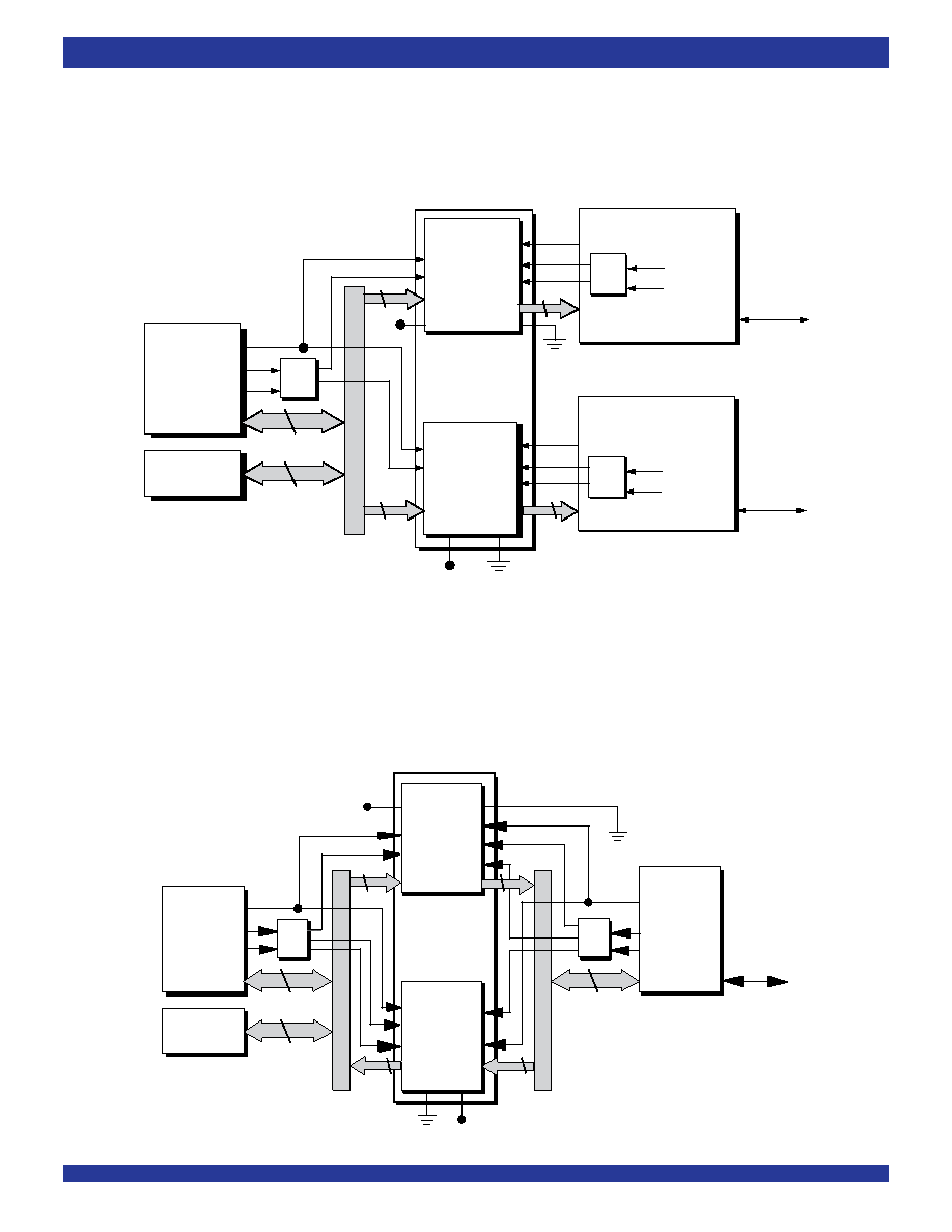
data according to type, sending one kind to FIFO A and the other kind to FIFO
B. Then, at the outputs, each data type is transferred to its appropriate
destination. Additional IDT72801/72811/72821/72831/72841/72851s permit
more than two priority levels. Priority buffering is particularly useful in network
applications.
TWO PRIORITY DATA BUFFER
CONFIGURATION
The two FIFOs contained in the IDT72801/72811/72821/72831/72841/
72851 can be used to prioritize two different types of data shared on a system
bus. When writing from the bus to the FIFO, control logic sorts the intermixed
Figure 16. Block Diagram of Two Priority Configuration
BIDIRECTIONAL CONFIGURATION
The two FIFOs of the IDT72801/72811/72821/72831/72841/72851 can
be used to buffer data flow in two directions. In the example that follows, a
processor can write data to a peripheral controller via FIFO A, and, in turn,
the peripheral controller can write the processor via FIFO B.
Figure 17. Block Diagram of Bidirectional Configuration
RAM ARRAY A
Processor
Data
DA0-DA8
QA0-QA8
OEA
RENA
Address
IDT
72801
72811
72821
72831
72841
72851
DB0-DB8
QB0-QB8
OEB2
WENB1
Control
Logic
RAM
9-bit
bus
RCLKA
WCLKB
Control
9
WCLKA
WENA1
RAM ARRAY B
RENB1
Clock
RCLKB
WENB2
RENB2
WENA2
RENA2
VCC
9
Voice Processing
Card
Data
I/O Data
Clock
Control
Logic
Address
Control
Image Processing
Card
Data
I/O Data
Clock
Control
Logic
Address
Control
3034 drw 17
RAM ARRAY A
Processor
Peripheral
Controller
Data
DA0-DA8
QA0-QA8
Data
OEA
RENA1
Address
I/O Data
IDT
72801
72811
72821
72831
72841
72851
DB0-DB8
QB0-QB8
OEB
WENB1
RAM
9-bit
bus
9-bit
bus
RCLKA
WCLKB
Control
9
WCLKA
WENA1
RAM ARRAY B
RENB1
Clock
RCLKB
DMA Clock
Control
Logic
Address
Control
9
WENB2
RENB2
WENA2 RENA2
VCC
3034 drw 18
Control
Logic
相關(guān)PDF資料 |
PDF描述 |
|---|---|
| 72821L15TF8 | 1K X 9 BI-DIRECTIONAL FIFO, 10 ns, PQFP64 |
| 72R99-P | 25 A, BARRIER STRIP TERMINAL BLOCK, 1 ROW, 1 DECK |
| 72R99-M | 25 A, BARRIER STRIP TERMINAL BLOCK, 1 ROW, 1 DECK |
| 72R99-59 | 25 A, BARRIER STRIP TERMINAL BLOCK, 1 ROW, 1 DECK |
| 72R99-49 | 25 A, BARRIER STRIP TERMINAL BLOCK, 1 ROW, 1 DECK |
相關(guān)代理商/技術(shù)參數(shù) |
參數(shù)描述 |
|---|---|
| 72841L10PF8 | 功能描述:先進(jìn)先出 RoHS:否 制造商:IDT 電路數(shù)量: 數(shù)據(jù)總線寬度:18 bit 總線定向:Unidirectional 存儲(chǔ)容量:4 Mbit 定時(shí)類型:Synchronous 組織:256 K x 18 最大時(shí)鐘頻率:100 MHz 訪問(wèn)時(shí)間:10 ns 電源電壓-最大:3.6 V 電源電壓-最小:6 V 最大工作電流:35 mA 最大工作溫度:+ 85 C 封裝 / 箱體:TQFP-80 封裝: |
| 72841L10PFG | 功能描述:先進(jìn)先出 RoHS:否 制造商:IDT 電路數(shù)量: 數(shù)據(jù)總線寬度:18 bit 總線定向:Unidirectional 存儲(chǔ)容量:4 Mbit 定時(shí)類型:Synchronous 組織:256 K x 18 最大時(shí)鐘頻率:100 MHz 訪問(wèn)時(shí)間:10 ns 電源電壓-最大:3.6 V 電源電壓-最小:6 V 最大工作電流:35 mA 最大工作溫度:+ 85 C 封裝 / 箱體:TQFP-80 封裝: |
| 72841L10PFG8 | 制造商:Integrated Device Technology Inc 功能描述:FIFO Mem Sync Quad Depth/Width Bi-Dir 4K x 9 x 2 64-Pin TQFP T/R 制造商:Integrated Device Technology Inc 功能描述:FIFO SYNC QUAD DEPTH/WIDTH BI-DIR 4KX9X2 64TQFP - Tape and Reel |
| 72841L10TF | 功能描述:先進(jìn)先出 RoHS:否 制造商:IDT 電路數(shù)量: 數(shù)據(jù)總線寬度:18 bit 總線定向:Unidirectional 存儲(chǔ)容量:4 Mbit 定時(shí)類型:Synchronous 組織:256 K x 18 最大時(shí)鐘頻率:100 MHz 訪問(wèn)時(shí)間:10 ns 電源電壓-最大:3.6 V 電源電壓-最小:6 V 最大工作電流:35 mA 最大工作溫度:+ 85 C 封裝 / 箱體:TQFP-80 封裝: |
| 72841L10TF8 | 制造商:Integrated Device Technology Inc 功能描述:FIFO Mem Sync Quad Depth/Width Bi-Dir 4K x 9 x 2 64-Pin STQFP T/R 制造商:Integrated Device Technology Inc 功能描述:FIFO SYNC QUAD DEPTH/WIDTH BI-DIR 4KX9X2 64TQFP - Tape and Reel |
發(fā)布緊急采購(gòu),3分鐘左右您將得到回復(fù)。