- 您現(xiàn)在的位置:買賣IC網(wǎng) > PDF目錄250211 > 71V3577YS75PF8 (INTEGRATED DEVICE TECHNOLOGY INC) 128K X 36 CACHE SRAM, 7.5 ns, PQFP100 PDF資料下載
參數(shù)資料
| 型號(hào): | 71V3577YS75PF8 |
| 廠商: | INTEGRATED DEVICE TECHNOLOGY INC |
| 元件分類: | SRAM |
| 英文描述: | 128K X 36 CACHE SRAM, 7.5 ns, PQFP100 |
| 封裝: | 14 X 20 MM, PLASTIC, TQFP-100 |
| 文件頁數(shù): | 8/22頁 |
| 文件大小: | 621K |
| 代理商: | 71V3577YS75PF8 |
6.42
16
IDT71V3577YS_79YS, IDT71V3577YSA_79YSA, 128K x 36, 256K x 18, 3.3V Synchronous SRAMs with
3.3V I/O, Flow-Through Outputs, Burst Counter, Single Cycle Deselect
Commercial and Industrial Temperature Ranges
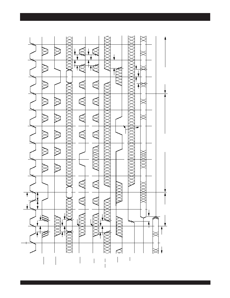
Timing Waveform of Write Cycle No. 2 - Byte Controlled (1,2,3)
A
D
R
E
S
C
L
K
A
D
S
P
A
D
S
C
tC
Y
C
tS
S
tH
S
tC
H
tC
L
tH
A
tS
A
x
A
y
tH
W
B
W
x
A
D
V
D
A
T
A
O
U
T
O
E
tH
C
tS
D
S
in
g
le
W
ri
te
B
u
rs
t
W
ri
te
I1
(A
x
)
I2
(A
y
)
I2
(A
y
)
I2
(A
z
)
tH
D
B
u
rs
t
R
e
a
d
E
x
te
n
d
e
d
B
u
rs
t
W
ri
te
tO
H
Z
D
A
T
A
IN
tS
A
V
tS
W
O
4
(A
w
)
C
E
,
C
S
1
tH
W
B
W
E
tS
W
(N
o
te
3
)
I1
(A
z
)
A
z
I4
(A
y
)
I1
(A
y
)
I4
(A
y
)
I3
(A
y
)
tS
C
B
W
E
is
ig
n
o
re
d
w
h
e
n
A
D
S
P
in
it
ia
te
s
a
c
y
c
le
a
n
d
is
s
a
m
p
le
d
o
n
th
e
n
e
x
t
c
y
c
le
ri
s
in
g
e
d
g
e
B
W
x
is
ig
n
o
re
d
w
h
e
n
A
D
S
P
in
it
ia
te
s
a
c
y
c
le
a
n
d
is
s
a
m
p
le
d
o
n
th
e
n
e
x
t
c
lo
c
k
ri
s
in
g
e
d
g
e
I3
(A
z
)
O
3
(A
w
)
6
4
5
0
d
rw
0
9
(A
D
V
H
IG
H
s
u
s
p
e
n
d
s
b
u
rs
t)
,
NOTES:
1.
ZZ
input
is
LOW,
GW
is
HIGH
and
LBO
is
Don't
Care
for
this
cycle.
2.
O4
(Aw)
represents
the
final
output
data
in
the
burst
sequence
of
the
base
address
Aw.
I1
(Ax)
represents
the
first
input
fr
om
the
external
address
Ax.
I1
(Ay)
represents
the
first
input
from
the
external
address
Ay;
I2
(Ay)
represents
the
next
input
data
in
the
burst
sequence
of
the
base
address
Ay,
etc.
where
A0
and
A1
are
advan
cing
for
the
four
word
burst
in
the
sequence
defined
by
the
state
of
the
LBO
input.
In
the
case
of
input
I2
(Ay)
this
data
is
valid
for
two
cycles
because
ADV
is
high
and
has
suspended
the
burst.
3.
C
S
0timing
transitions
are
identical
but
inverted
to
the
CE
and
CS
1
signals.
For
example,
when
CE
and
CS
1are
LOW
on
this
waveform,
CS
0is
HIGH.
相關(guān)PDF資料 |
PDF描述 |
|---|---|
| 7P24FLV251C25 | 12M X 16 FLASH 3V PROM CARD, 250 ns, XMA68 |
| 7P24FLV280I15 | 12M X 16 FLASH 3V PROM CARD, 150 ns, XMA68 |
| 7P24FLV282I25 | 12M X 16 FLASH 3V PROM CARD, 250 ns, XMA68 |
| 7P24FLV551I15 | 12M X 16 FLASH 3V PROM CARD, 150 ns, XMA68 |
| 7P24FLV560C15 | 12M X 16 FLASH 3V PROM CARD, 150 ns, XMA68 |
相關(guān)代理商/技術(shù)參數(shù) |
參數(shù)描述 |
|---|---|
| 71V3577YS85PFG | 功能描述:IC SRAM 4.5MBIT 8.5NS 100TQFP 制造商:idt, integrated device technology inc 系列:- 包裝:托盤 零件狀態(tài):過期 格式 - 存儲(chǔ)器:RAM 存儲(chǔ)器類型:SRAM - 同步 存儲(chǔ)容量:4.5M(128K x 36) 速度:8.5ns 接口:并聯(lián) 電壓 - 電源:3.135 V ~ 3.465 V 工作溫度:0°C ~ 70°C(TA) 封裝/外殼:100-LQFP 供應(yīng)商器件封裝:100-TQFP(14x20) 標(biāo)準(zhǔn)包裝:72 |
| 71V3578S133PF | 制造商:Integrated Device Technology Inc 功能描述:SRAM CHIP SYNC SINGLE 3.3V 4.5M-BIT 256K X 18 4.2NS - Trays 制造商:Integrated Device Technology Inc 功能描述:IDT 71V3578S133PF, SRAM Chip Sync Single 3.3V 4.5M-Bit 256K x 18 4.2ns 100-Pin TQFP |
| 71V3578S133PFG | 功能描述:靜態(tài)隨機(jī)存取存儲(chǔ)器 256Kx18 SYNC 3.3V FLOW-THROUGH 靜態(tài)隨機(jī)存取存儲(chǔ)器 RoHS:否 制造商:Cypress Semiconductor 存儲(chǔ)容量:16 Mbit 組織:1 M x 16 訪問時(shí)間:55 ns 電源電壓-最大:3.6 V 電源電壓-最小:2.2 V 最大工作電流:22 uA 最大工作溫度:+ 85 C 最小工作溫度:- 40 C 安裝風(fēng)格:SMD/SMT 封裝 / 箱體:TSOP-48 封裝:Tray |
| 71V3578S133PFG8 | 功能描述:靜態(tài)隨機(jī)存取存儲(chǔ)器 256Kx18 SYNC 3.3V FLOW-THROUGH 靜態(tài)隨機(jī)存取存儲(chǔ)器 RoHS:否 制造商:Cypress Semiconductor 存儲(chǔ)容量:16 Mbit 組織:1 M x 16 訪問時(shí)間:55 ns 電源電壓-最大:3.6 V 電源電壓-最小:2.2 V 最大工作電流:22 uA 最大工作溫度:+ 85 C 最小工作溫度:- 40 C 安裝風(fēng)格:SMD/SMT 封裝 / 箱體:TSOP-48 封裝:Tray |
| 71V3578S133PFGI | 功能描述:靜態(tài)隨機(jī)存取存儲(chǔ)器 256Kx18 SYNC 3.3V FLOW-THROUGH 靜態(tài)隨機(jī)存取存儲(chǔ)器 RoHS:否 制造商:Cypress Semiconductor 存儲(chǔ)容量:16 Mbit 組織:1 M x 16 訪問時(shí)間:55 ns 電源電壓-最大:3.6 V 電源電壓-最小:2.2 V 最大工作電流:22 uA 最大工作溫度:+ 85 C 最小工作溫度:- 40 C 安裝風(fēng)格:SMD/SMT 封裝 / 箱體:TSOP-48 封裝:Tray |
發(fā)布緊急采購,3分鐘左右您將得到回復(fù)。