- 您現(xiàn)在的位置:買賣IC網(wǎng) > PDF目錄371435 > 28F1604C3 (Intel Corp.) 3 Volt Advanced+ Stacked Chip Scale Package Memory(3V閃速存儲(chǔ)器和靜態(tài)存儲(chǔ)器) PDF資料下載
參數(shù)資料
| 型號(hào): | 28F1604C3 |
| 廠商: | Intel Corp. |
| 英文描述: | 3 Volt Advanced+ Stacked Chip Scale Package Memory(3V閃速存儲(chǔ)器和靜態(tài)存儲(chǔ)器) |
| 中文描述: | 3伏高級(jí)堆疊芯片級(jí)封裝存儲(chǔ)器(3V的閃速存儲(chǔ)器和靜態(tài)存儲(chǔ)器) |
| 文件頁數(shù): | 27/64頁 |
| 文件大小: | 927K |
| 代理商: | 28F1604C3 |
第1頁第2頁第3頁第4頁第5頁第6頁第7頁第8頁第9頁第10頁第11頁第12頁第13頁第14頁第15頁第16頁第17頁第18頁第19頁第20頁第21頁第22頁第23頁第24頁第25頁第26頁當(dāng)前第27頁第28頁第29頁第30頁第31頁第32頁第33頁第34頁第35頁第36頁第37頁第38頁第39頁第40頁第41頁第42頁第43頁第44頁第45頁第46頁第47頁第48頁第49頁第50頁第51頁第52頁第53頁第54頁第55頁第56頁第57頁第58頁第59頁第60頁第61頁第62頁第63頁第64頁
28F1602C3, 28F1604C3, 28F3204C3
Preliminary
21
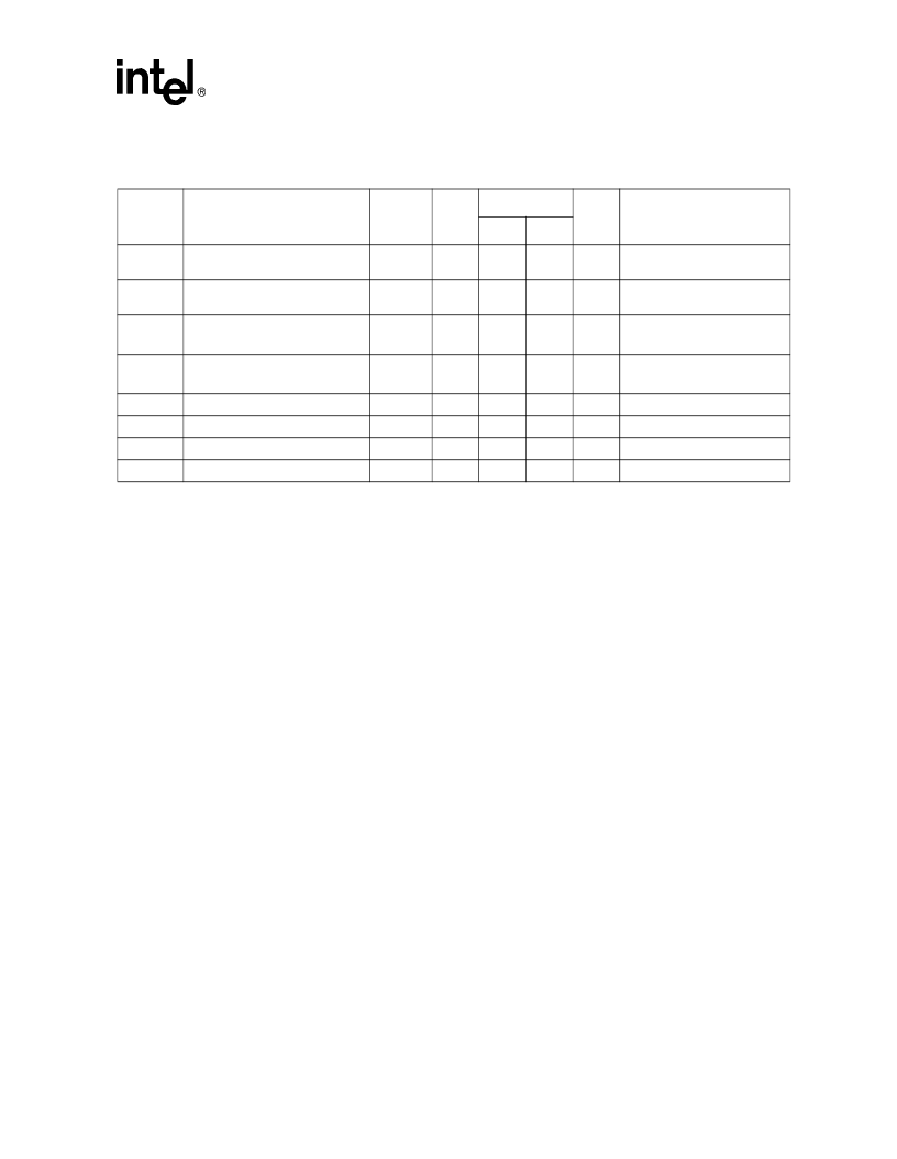
NOTES:
1. All currents are in RMS unless otherwise noted. Typical values at nominal F-V
/S-V
, T
= +25 °C.
2. I
and I
CCWS
are specified with device de-selected. If device is read while in erase suspend, current draw
is sum of I
CCES
and I
CCR
. If the device is read while in program suspend, current draw is the sum of I
CCWS
and I
.
3. Erase and Program are inhibited when F-V
PP
< V
PPLK
and not guaranteed outside the valid F-V
PP
ranges of
V
and V
.
4. Sampled, not 100% tested.
5. Automatic Power Savings (APS) reduces I
CCR
to approximately standby levels in static operation (CMOS
inputs).
6. Applying F-V
= 11.4 V–12.6 V during program/erase can only be done for a maximum of 1000 cycles on
the main blocks and 2500 cycles on the parameter blocks. F-V
PP
may be connected to 12 V for a total of 80
hours maximum. See
Section 3.9.1
for details.
DC Characteristics, Continued
Symbol
Parameter
Device
Note
2.7 V – 3.3 V
Unit
Test Conditions
Min
Max
V
IL
Input Low Voltage
Flash/
SRAM
–
0.2
0.6
V
V
IH
Input High Voltage
Flash/
SRAM
2.2
V
+0.2
V
V
OL
Output Low Voltage
Flash/
SRAM
7
–0.10
0.10
V
F-V
CC
/S-V
CC
= V
CC1
Min
I
OL
= 100
μ
A
V
OH
Output High Voltage
Flash/
SRAM
7
V
–
0.1
V
F-V
CC
/S-V
CC
= V
CC1
Min
I
OH
= –100
μ
A
V
PPLK
F-V
PP
Lock-Out Voltage
Flash
3
1.0
V
Complete Write Protection
V
PP1
F-V
PP
during Program / Erase
Flash
3
1.65
3.3
V
V
PP2
Operations
3,6
11.4
12.6
V
LKO
V
CC
Prog/Erase Lock Voltage
Flash
1.5
V
發(fā)布緊急采購,3分鐘左右您將得到回復(fù)。