- 您現(xiàn)在的位置:買賣IC網(wǎng) > PDF目錄371435 > 28F128 (Intel Corp.) 3 Volt Intel StrataFlash Memory PDF資料下載
參數(shù)資料
| 型號(hào): | 28F128 |
| 廠商: | Intel Corp. |
| 英文描述: | 3 Volt Intel StrataFlash Memory |
| 中文描述: | 3伏特英特爾StrataFlash存儲(chǔ)器 |
| 文件頁數(shù): | 49/58頁 |
| 文件大小: | 380K |
| 代理商: | 28F128 |
第1頁第2頁第3頁第4頁第5頁第6頁第7頁第8頁第9頁第10頁第11頁第12頁第13頁第14頁第15頁第16頁第17頁第18頁第19頁第20頁第21頁第22頁第23頁第24頁第25頁第26頁第27頁第28頁第29頁第30頁第31頁第32頁第33頁第34頁第35頁第36頁第37頁第38頁第39頁第40頁第41頁第42頁第43頁第44頁第45頁第46頁第47頁第48頁當(dāng)前第49頁第50頁第51頁第52頁第53頁第54頁第55頁第56頁第57頁第58頁
28F128J3A, 28F640J3A, 28F320J3A
Preliminary
43
DC Characteristics, Continued
NOTES:
1. All currents are in RMS unless otherwise noted. These currents are valid for all product versions (packages
and speeds). Contact Intel
’
s Application Support Hotline or your local sales office for information about typical
specifications.
2. Includes STS.
3. CMOS inputs are either V
CC
± 0.2 V or GND ± 0.2 V. TTL inputs are either V
IL
or V
IH
.
4. Current values are specified over the temperature range (0
°
C to 70
°
C) and may increase slightly at
–
25
°
C.
5. Sampled, not 100% tested.
6. I
CCWS
and I
CCES
are specified with the device de-selected. If the device is read or written while in erase
suspend mode, the device
’
s current draw is I
CCR
or I
CCW
.
7. Block erases, programming, and lock-bit configurations are inhibited when V
PEN
≤
V
PENLK
, and not
guaranteed in the range between V
PENLK
(max) and V
PENH
(min), and above V
PENH
(max).
8. Typically, V
PEN
is connected to V
CC
(2.7 V
–
3.6 V).
9. Block erases, programming, and lock-bit configurations are inhibited when V
CC
< V
LKO
, and not guaranteed
in the range between V
LKO
(min) and V
CC
(min), and above V
CC
(max).
NOTE:
AC test inputs are driven at V
for a Logic "1" and 0.0 V for a Logic "0." Input timing begins, and
output timing ends, at V
CCQ
/2 V (50% of V
CCQ
). Input rise and fall times (10% to 90%) < 5 ns.
Symbol
Parameter
Notes
Min
Max
Unit
Test Conditions
V
IL
Input Low Voltage
5
–
0.5
0.8
V
V
IH
Input High Voltage
5
2.0
V
CCQ
+ 0.5
V
V
OL
Output Low Voltage
2,5
0.4
V
V
CCQ
= V
CCQ2/3
Min
I
OL
= 2 mA
0.2
V
V
CCQ
= V
CCQ2/3
Min
I
OL
= 100 μA
V
OH
Output High Voltage
2,5
0.85
×
V
CCQ
V
V
CCQ
= V
CCQ
Min
I
OH
=
–
2.5 mA
V
CCQ
–
0.2
V
V
CCQ
= V
CCQ
Min
I
OH
=
–
100 μA
V
PENLK
V
PEN
Lockout during Program,
Erase and Lock-Bit Operations
5,7,8
2.0
V
V
PENH
V
PEN
during Block Erase,
Program, or Lock-Bit Operations
7,8
2.7
3.6
V
V
LKO
V
CC
Lockout Voltage
9
2.0
V
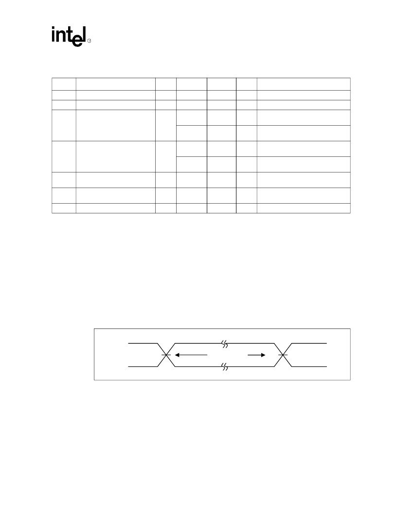
Figure 15. Transient Input/Output Reference Waveform for V
CCQ
= 3.0 V
–
3.6 V or
V
CCQ
= 2.7 V
–
3.6 V
Output
Test Points
Input V
CCQ
/2
0.0
V
CCQ
V
CCQ
/2
相關(guān)PDF資料 |
PDF描述 |
|---|---|
| 28F1602C3 | 3 Volt Advanced+ Stacked Chip Scale Package Memory(3V閃速存儲(chǔ)器和靜態(tài)存儲(chǔ)器) |
| 28F3204C3 | 3 V Advanced+ Stacked Chip Scale Package Memory(3V高級(jí)堆芯片封裝存儲(chǔ)器) |
| 28F1604C3 | 3 Volt Advanced+ Stacked Chip Scale Package Memory(3V閃速存儲(chǔ)器和靜態(tài)存儲(chǔ)器) |
| 28F160C18 | 1.8V Advanced+ Boot Block Flash Memory(1.8V高級(jí)引導(dǎo)塊閃速存儲(chǔ)器) |
| 28F160C2 | 2.4V Advanced+ Boot Block Flash Memory(2.4V高級(jí)引導(dǎo)塊閃速存儲(chǔ)器) |
相關(guān)代理商/技術(shù)參數(shù) |
參數(shù)描述 |
|---|---|
| 28F128J3A | 制造商:INTEL 制造商全稱:Intel Corporation 功能描述:3 Volt Intel StrataFlash Memory |
| 28F128J3A150 | 制造商: 功能描述: 制造商:INTELC 功能描述: 制造商:undefined 功能描述: |
| 28F128J3A-150 | 制造商: 功能描述: 制造商:undefined 功能描述: |
| 28F128J3D75 | 制造商: 功能描述: 制造商:Intel 功能描述: |
| 28F128J3FS-12ET | 制造商: 功能描述: 制造商:undefined 功能描述: |
發(fā)布緊急采購,3分鐘左右您將得到回復(fù)。