- 您現(xiàn)在的位置:買賣IC網(wǎng) > PDF目錄371435 > 28F128 (Intel Corp.) 3 Volt Intel StrataFlash Memory PDF資料下載
參數(shù)資料
| 型號: | 28F128 |
| 廠商: | Intel Corp. |
| 英文描述: | 3 Volt Intel StrataFlash Memory |
| 中文描述: | 3伏特英特爾StrataFlash存儲(chǔ)器 |
| 文件頁數(shù): | 26/58頁 |
| 文件大小: | 380K |
| 代理商: | 28F128 |
第1頁第2頁第3頁第4頁第5頁第6頁第7頁第8頁第9頁第10頁第11頁第12頁第13頁第14頁第15頁第16頁第17頁第18頁第19頁第20頁第21頁第22頁第23頁第24頁第25頁當(dāng)前第26頁第27頁第28頁第29頁第30頁第31頁第32頁第33頁第34頁第35頁第36頁第37頁第38頁第39頁第40頁第41頁第42頁第43頁第44頁第45頁第46頁第47頁第48頁第49頁第50頁第51頁第52頁第53頁第54頁第55頁第56頁第57頁第58頁
28F128J3A, 28F640J3A, 28F320J3A
20
Preliminary
NOTES:
1. A
0
is not used in either x8 or x16 modes when obtaining the identifier codes. The lowest order address line is
A
1
. Data is always presented on the low byte in x16 mode (upper byte contains 00h).
2. X selects the specific block
’
s lock configuration code. See
Figure 5
for the device identifier code memory
map.
4.4
Read Status Register Command
The status register may be read to determine when a block erase, program, or lock-bit configuration
is complete and whether the operation completed successfully. It may be read at any time by
writing the Read Status Register command. After writing this command, all subsequent read
operations output data from the status register until another valid command is written. Page-mode
reads are not supported in this read mode. The status register contents are latched on the falling
edge of OE# or the first edge of CE
0
, CE
1
, or CE
2
that enables the device (see
Table 2,
“
Chip
Enable Truth Table
”
on page 7
). OE# must toggle to V
IH
or the device must be disabled (see
Table
2
) before further reads to update the status register latch. The Read Status Register command
functions independently of the V
PEN
voltage.
During a program, block erase, set lock-bit, or clear lock-bit command sequence, only SR.7 is valid
until the Write State Machine completes or suspends the operation. Device I/O pins DQ
0
–
DQ
6
and
DQ
8
–
DQ
15
are placed in a high-impedance state. When the operation completes or suspends
(check status register bit 7), all contents of the status register are valid when read.
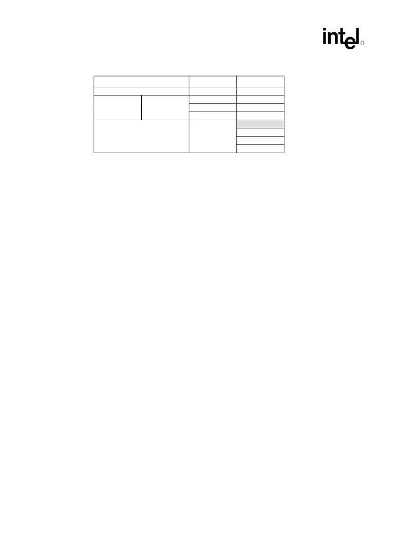
Table 15. Identifier Codes
Code
Address
(1)
Data
Manufacture Code
Device Code
00000
00001
00001
00001
X
0002
(2)
(00) 89
(00) 16
(00) 17
(00) 18
32-Mbit
64-Mbit
128-Mbit
Block Lock Configuration
Block Is Unlocked
Block Is Locked
Reserved for Future Use
DQ
0
= 0
DQ
0
= 1
DQ
1
–
7
相關(guān)PDF資料 |
PDF描述 |
|---|---|
| 28F1602C3 | 3 Volt Advanced+ Stacked Chip Scale Package Memory(3V閃速存儲(chǔ)器和靜態(tài)存儲(chǔ)器) |
| 28F3204C3 | 3 V Advanced+ Stacked Chip Scale Package Memory(3V高級堆芯片封裝存儲(chǔ)器) |
| 28F1604C3 | 3 Volt Advanced+ Stacked Chip Scale Package Memory(3V閃速存儲(chǔ)器和靜態(tài)存儲(chǔ)器) |
| 28F160C18 | 1.8V Advanced+ Boot Block Flash Memory(1.8V高級引導(dǎo)塊閃速存儲(chǔ)器) |
| 28F160C2 | 2.4V Advanced+ Boot Block Flash Memory(2.4V高級引導(dǎo)塊閃速存儲(chǔ)器) |
相關(guān)代理商/技術(shù)參數(shù) |
參數(shù)描述 |
|---|---|
| 28F128J3A | 制造商:INTEL 制造商全稱:Intel Corporation 功能描述:3 Volt Intel StrataFlash Memory |
| 28F128J3A150 | 制造商: 功能描述: 制造商:INTELC 功能描述: 制造商:undefined 功能描述: |
| 28F128J3A-150 | 制造商: 功能描述: 制造商:undefined 功能描述: |
| 28F128J3D75 | 制造商: 功能描述: 制造商:Intel 功能描述: |
| 28F128J3FS-12ET | 制造商: 功能描述: 制造商:undefined 功能描述: |
發(fā)布緊急采購,3分鐘左右您將得到回復(fù)。