- 您現(xiàn)在的位置:買賣IC網(wǎng) > PDF目錄2019 > XRT71D00IQ-F (Exar Corporation)IC JITTER ATTENUATOR SGL 32TQFP PDF資料下載
參數(shù)資料
| 型號: | XRT71D00IQ-F |
| 廠商: | Exar Corporation |
| 文件頁數(shù): | 26/26頁 |
| 文件大小: | 0K |
| 描述: | IC JITTER ATTENUATOR SGL 32TQFP |
| 標準包裝: | 250 |
| 類型: | * |
| PLL: | 是 |
| 輸入: | 時鐘 |
| 輸出: | 時鐘 |
| 電路數(shù): | 1 |
| 比率 - 輸入:輸出: | 3:2 |
| 差分 - 輸入:輸出: | 無/無 |
| 頻率 - 最大: | 44.736MHz |
| 除法器/乘法器: | 無/無 |
| 電源電壓: | 3.135 V ~ 5.25 V |
| 工作溫度: | -40°C ~ 85°C |
| 安裝類型: | 表面貼裝 |
| 封裝/外殼: | 32-LQFP |
| 供應商設備封裝: | 32-TQFP(7x7) |
| 包裝: | 托盤 |
á
XRT71D00
E3/DS3/STS-1 JITTER ATTENUATOR
REV. 1.2.0
8
26
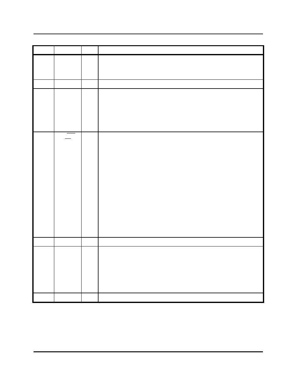
RRPOS
O
Receive Positive Data (De-Jittered) Output.
Data which is input via the “RPOS” input pin will be updated on the rising or falling
edge of RRClk (see pin 9), depending upon the state of the ClkES input pin (or bit-field
setting).
27
VDD
***
Digital Positive Supply Voltage: 3.3V or 5.0V ± 5%
28
Ch_Addr_0
I
Channel Addr_0 Assignment Input.
This input pin, along with pin 15 permits the user to assign a “Channel Address” to the
XRT71D00.
NOTES
1. A detailed discussion on “Channel Assignment” is presented in Section _.
2. This input pin is only active whenever the XRT71D00 device has been config-
ured to operate in the “Host” Mode.
29
E3/DS3
(CS)
I
E3/DS3 Select Input/Chip Select Input:
The function of this pin depends on whether the XRT71D00 is configured in Host or
Hardware mode.
Hardware Mode—E3/DS3* Select Input:
This pin along with the STS-1 mode select pin (pin 8) selects the operating mode. A
table relating the settings of these two input pins to the operatintg mode of the
XRT71D00 device is given below.:
STS-1
E3/DS3*
XRT71D00 Operating Mode
0
DS3 (44.736 MHz)
0
1
E3 (34.368 MHz)
1
0
STS-1 (51.84 MHz)
1
E3 (34.368 MHz)
NOTE: For SONET De-synchronization applications, the user should configure the
XRT71D00 device to operate in the DS3 Mode.
HOST Mode—Chip Select Input:
The local microprocessor must assert this input pin (e.g., set it to “0”) in order to enable
communication with the XRT71D00 device, via the MIcroprocessor Serial Interface.
30
VDD
***
Digital Positive Supply Voltage: 3.3V or 5.0V ± 5%
31
RPOS
I
Receive Positive Data (Jittery) Input.
Data that is input on this pin is sampled on either the rising or falling edge of RClk
depending on the setting of the ClkES pin (pin 10). This data will ultimately be output
via the “RRPOS” output pin.
If ClkES is “high”, then RPOS will be sampled on the falling edge of RClk.
If ClkES is “l(fā)ow”, then RPOS will be sampled on the rising edge of RClk.
NOTE: For “Jitter Attenuation” Applications, this pin is typically connected to the
“RPOS” output pin of the corresponding LIU IC.
32
NC
***
This pin is not connected internally.
PIN DESCRIPTION
PIN #NAME
TYPE
DESCRIPTION
相關(guān)PDF資料 |
PDF描述 |
|---|---|
| XRT71D03IV-F | IC JITTER ATTENUATOR 3CH 64TQFP |
| XRT71D04IV | IC JITTER ATTENUATOR 4CH 80TQFP |
| XRT8000IP-F | IC WAN CLOCK E1/E1 DUAL 18PDIP |
| XRT8001IP-F | IC WAN CLOCK E1/E1 DUAL 18PDIP |
| XRT8010IL-F | IC CLK MULTIPLR LVDS 16QFN |
相關(guān)代理商/技術(shù)參數(shù) |
參數(shù)描述 |
|---|---|
| XRT71D00IQTR-F | 功能描述:時鐘合成器/抖動清除器 DS3/E3/STS-1Jit Attn 3.3/5.0V 1 CH 1 CHIP RoHS:否 制造商:Skyworks Solutions, Inc. 輸出端數(shù)量: 輸出電平: 最大輸出頻率: 輸入電平: 最大輸入頻率:6.1 GHz 電源電壓-最大:3.3 V 電源電壓-最小:2.7 V 封裝 / 箱體:TSSOP-28 封裝:Reel |
| XRT71D03 | 制造商:EXAR 制造商全稱:EXAR 功能描述:3 CHANNEL E3/DS3/STS-1 JITTER ATTENUATOR |
| XRT71D03ES | 功能描述:時鐘合成器/抖動清除器 3CH T3/E3JA w/T73LC03A RoHS:否 制造商:Skyworks Solutions, Inc. 輸出端數(shù)量: 輸出電平: 最大輸出頻率: 輸入電平: 最大輸入頻率:6.1 GHz 電源電壓-最大:3.3 V 電源電壓-最小:2.7 V 封裝 / 箱體:TSSOP-28 封裝:Reel |
| XRT71D03IV | 制造商:EXAR 制造商全稱:EXAR 功能描述:3 CHANNEL E3/DS3/STS-1 JITTER ATTENUATOR |
| XRT71D03IV-F | 功能描述:時鐘合成器/抖動清除器 RoHS:否 制造商:Skyworks Solutions, Inc. 輸出端數(shù)量: 輸出電平: 最大輸出頻率: 輸入電平: 最大輸入頻率:6.1 GHz 電源電壓-最大:3.3 V 電源電壓-最小:2.7 V 封裝 / 箱體:TSSOP-28 封裝:Reel |
發(fā)布緊急采購,3分鐘左右您將得到回復。