- 您現(xiàn)在的位置:買賣IC網(wǎng) > PDF目錄16427 > XR17V258IV-0A-EVB (Exar Corporation)EVAL BOARD FOR XR17V258 144LQFP PDF資料下載
參數(shù)資料
| 型號(hào): | XR17V258IV-0A-EVB |
| 廠商: | Exar Corporation |
| 文件頁(yè)數(shù): | 56/69頁(yè) |
| 文件大小: | 0K |
| 描述: | EVAL BOARD FOR XR17V258 144LQFP |
| 標(biāo)準(zhǔn)包裝: | 1 |
| 系列: | * |
第1頁(yè)第2頁(yè)第3頁(yè)第4頁(yè)第5頁(yè)第6頁(yè)第7頁(yè)第8頁(yè)第9頁(yè)第10頁(yè)第11頁(yè)第12頁(yè)第13頁(yè)第14頁(yè)第15頁(yè)第16頁(yè)第17頁(yè)第18頁(yè)第19頁(yè)第20頁(yè)第21頁(yè)第22頁(yè)第23頁(yè)第24頁(yè)第25頁(yè)第26頁(yè)第27頁(yè)第28頁(yè)第29頁(yè)第30頁(yè)第31頁(yè)第32頁(yè)第33頁(yè)第34頁(yè)第35頁(yè)第36頁(yè)第37頁(yè)第38頁(yè)第39頁(yè)第40頁(yè)第41頁(yè)第42頁(yè)第43頁(yè)第44頁(yè)第45頁(yè)第46頁(yè)第47頁(yè)第48頁(yè)第49頁(yè)第50頁(yè)第51頁(yè)第52頁(yè)第53頁(yè)第54頁(yè)第55頁(yè)當(dāng)前第56頁(yè)第57頁(yè)第58頁(yè)第59頁(yè)第60頁(yè)第61頁(yè)第62頁(yè)第63頁(yè)第64頁(yè)第65頁(yè)第66頁(yè)第67頁(yè)第68頁(yè)第69頁(yè)
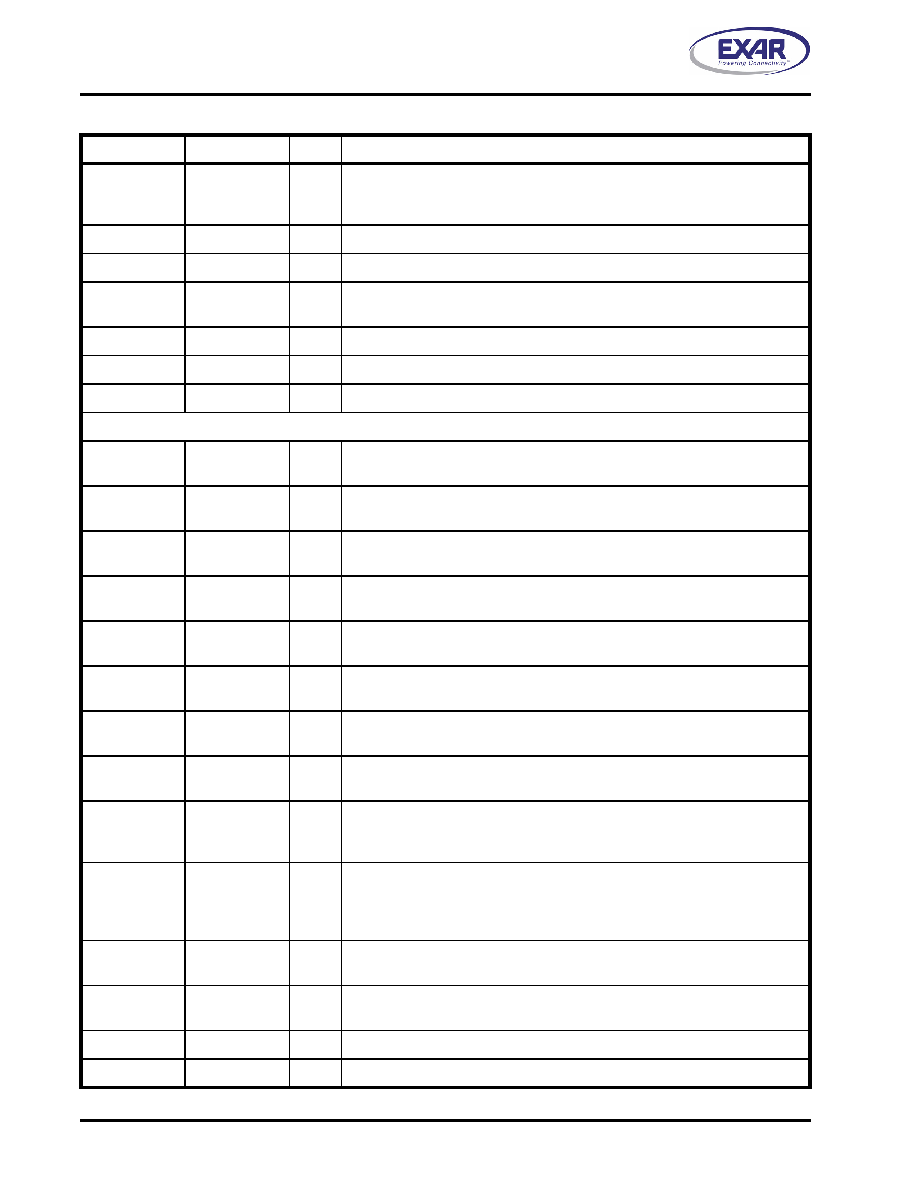
XR17V258
6
66MHZ PCI BUS OCTAL UART WITH POWER MANAGEMENT SUPPORT
REV. 1.0.2
RX7
47
I
UART channel 7 Receive Data or infrared receive data. Normal RXD input
idles at HIGH condition. The infrared pulses can be inverted prior to decoding
by setting FCTR bit [4].
RTS7#
52
O
UART channel 7 Request to Send or general purpose output (active LOW).
CTS7#
48
I
UART channel 7 Clear to Send or general purpose input (active LOW).
DTR7#
53
O
UART channel 7 Data Terminal Ready or general purpose output (active
LOW).
DSR7#
49
I
UART channel 7 Data Set Ready or general purpose input (active LOW).
CD7#
50
I
UART channel 7 Carrier Detect or general purpose input (active LOW).
RI7#
51
I
UART channel 7 Ring Indicator or general purpose input (active LOW).
ANCILLARY SIGNALS
MPIO0
108
I/O
Multi-purpose input/output 0. The function of this pin is defined thru the Con-
figuration Register MPIOSEL, MPIOLVL, MPIOINV, MPIO3T and MPIOINT
MPIO1
107
I/O
Multi-purpose input/output 1. The function of this pin is defined thru the Con-
figuration Register MPIOSEL, MPIOLVL, MPIOINV, MPIO3T and MPIOINT.
MPIO2
74
I/O
Multi-purpose input/output 2. The function of this pin is defined thru the Con-
figuration Register MPIOSEL, MPIOLVL, MPIOINV, MPIO3T and MPIOINT.
MPIO3
73
I/O
Multi-purpose input/output 3. The function of this pin is defined thru the Con-
figuration Register MPIOSEL, MPIOLVL, MPIOINV, MPIO3T and MPIOINT.
MPIO4
68
I/O
Multi-purpose input/output 4. The function of this pin is defined thru the Con-
figuration Register MPIOSEL, MPIOLVL, MPIOINV, MPIO3T and MPIOINT.
MPIO5
67
I/O
Multi-purpose input/output 5. The function of this pin is defined thru the Con-
figuration Register MPIOSEL, MPIOLVL, MPIOINV, MPIO3T and MPIOINT.
MPIO6
66
I/O
Multi-purpose input/output 6. The function of this pin is defined thru the Con-
figuration Register MPIOSEL, MPIOLVL, MPIOINV, MPIO3T and MPIOINT.
MPIO7
65
I/O
Multi-purpose input/output 7. The function of this pin is defined thru the Con-
figuration Register MPIOSEL, MPIOLVL, MPIOINV, MPIO3T and MPIOINT.
EECK
116
O
Serial clock to EEPROM. An internal clock of CLK divide by 256 is used for
reading the vendor and sub-vendor ID during power up or reset. However, it
can be manually clocked thru the Configuration Register REGB.
EECS
115
O
Chip select to a EEPROM device like 93C46. It is manually selectable thru
the Configuration Register REGB. Requires a pull-up 4.7K ohm resistor for
external sensing of EEPROM during power up. See DAN112 for further
details.
EEDI
114
O
Write data to EEPROM device. It is manually accessible thru the Configura-
tion Register REGB.
EEDO
113
I
Read data from EEPROM device. It is manually accessible thru the Configu-
ration Register REGB.
XTAL1
110
I
Crystal or external clock input.
XTAL2
109
O
Crystal or buffered clock output.
PIN DESCRIPTIONS
NAME
PIN #TYPE
DESCRIPTION
相關(guān)PDF資料 |
PDF描述 |
|---|---|
| GCC10DRYN-S734 | CONN EDGECARD 20POS DIP .100 SLD |
| VI-B1Y-EV | CONVERTER MOD DC/DC 3.3V 99W |
| 155880-000 | SOLDER SLEEVE 11MM DIA SHIELD |
| VI-2VR-EX | CONVERTER MOD DC/DC 7.5V 75W |
| VI-2VP-EX | CONVERTER MOD DC/DC 13.8V 75W |
相關(guān)代理商/技術(shù)參數(shù) |
參數(shù)描述 |
|---|---|
| XR17V258IVF | 制造商:Exar Corporation 功能描述: |
| XR17V258IV-F | 功能描述:UART 接口集成電路 66MHz Octal PCI UART RoHS:否 制造商:Texas Instruments 通道數(shù)量:2 數(shù)據(jù)速率:3 Mbps 電源電壓-最大:3.6 V 電源電壓-最小:2.7 V 電源電流:20 mA 最大工作溫度:+ 85 C 最小工作溫度:- 40 C 封裝 / 箱體:LQFP-48 封裝:Reel |
| XR17V258IVTR-F | 功能描述:UART 接口集成電路 66MHz Octal PCI UART RoHS:否 制造商:Texas Instruments 通道數(shù)量:2 數(shù)據(jù)速率:3 Mbps 電源電壓-最大:3.6 V 電源電壓-最小:2.7 V 電源電流:20 mA 最大工作溫度:+ 85 C 最小工作溫度:- 40 C 封裝 / 箱體:LQFP-48 封裝:Reel |
| XR17V352 | 制造商:EXAR 制造商全稱:EXAR 功能描述:HIGH PERFORMANCE DUAL PCI EXPRESS UART |
| XR17V352IB-0A-EVB | 功能描述:界面開發(fā)工具 Eval Board for XR17V352IB Series RoHS:否 制造商:Bourns 產(chǎn)品:Evaluation Boards 類型:RS-485 工具用于評(píng)估:ADM3485E 接口類型:RS-485 工作電源電壓:3.3 V |
發(fā)布緊急采購(gòu),3分鐘左右您將得到回復(fù)。