- 您現(xiàn)在的位置:買賣IC網(wǎng) > PDF目錄16524 > XR16V2552IL-0B-EB (Exar Corporation)EVAL BOARD FOR V2552 32QFN PDF資料下載
參數(shù)資料
| 型號: | XR16V2552IL-0B-EB |
| 廠商: | Exar Corporation |
| 文件頁數(shù): | 44/46頁 |
| 文件大小: | 0K |
| 描述: | EVAL BOARD FOR V2552 32QFN |
| 標準包裝: | 1 |
| 系列: | * |
第1頁第2頁第3頁第4頁第5頁第6頁第7頁第8頁第9頁第10頁第11頁第12頁第13頁第14頁第15頁第16頁第17頁第18頁第19頁第20頁第21頁第22頁第23頁第24頁第25頁第26頁第27頁第28頁第29頁第30頁第31頁第32頁第33頁第34頁第35頁第36頁第37頁第38頁第39頁第40頁第41頁第42頁第43頁當前第44頁第45頁第46頁
XR16V2552
7
REV. 1.0.3
HIGH PERFORMANCE DUART WITH 16-BYTE FIFO
2.0 FUNCTIONAL DESCRIPTIONS
2.1
CPU Interface
The CPU interface is 8 data bits wide with 3 address lines and control signals to execute data bus read and
write transactions. The 2552 data interface supports the Intel compatible types of CPUs and it is compatible to
the industry standard 16C550 UART. No clock (oscillator nor external clock) is required to operate a data bus
transaction. Each bus cycle is asynchronous using CS#, IOR# and IOW# signals. Both UART channels share
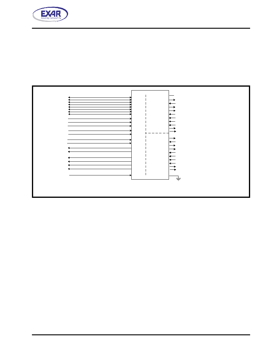
the same data bus for host operations. The data bus interconnections are shown in Figure 3
FIGURE 3. XR16V2552 DATA BUS INTERCONNECTIONS
VCC
(OP2A#)
DSRA#
CTSA#
RTSA#
DTRA#
RXA
TXA
RIA#
CDA#
(OP2B#)
DSRB#
CTSB#
RTSB#
DTRB#
RXB
TXB
RIB#
CDB#
GND
A0
A1
A2
UART_CS#
UART_CHSEL
IOR#
IOW#
D0
D1
D2
D3
D4
D5
D6
D7
A0
A1
A2
CS#
CHSEL
D0
D1
D2
D3
D4
D5
D6
D7
IOR#
IOW#
UART
Channel A
UART
Channel B
UART_INTB
UART_INTA
INTB
INTA
(RXRDYA#)
TXRDYA#
(RXRDYA#)
TXRDYA#
(RXRDYB#)
TXRDYB#
(RXRDYB#)
TXRDYB#
UART_RESET
RESET
Serial Interface of
RS-232, RS-422
Serial Interface of
RS-232, RS-422
(BAUDOUTB#)
(BAUDOUTA#)
Pins in parentheses become available through the MF# pin. MF# A/B becomes RXRDY# A/B when AFR[2:1] = '10'. MF# A/B becomes OP2# A/B
when AFR[2:1] = '00'. MF# A/B becomes BAUDOUT# A/B when AFR[1:0] = '01'.
2.2
5-Volt Tolerant Inputs
The V2552 can accept up to 5V inputs even when operating at 3.3V or 2.5V. But note that if the V2552 is
operating at 2.5V, its VOH may not be high enough to meet the requirements of the VIH of a CPU or a serial
transceiver that is operating at 5V.
2.3
Device Reset
The RESET input resets the internal registers and the serial interface outputs in both channels to their default
state (see Table 15). An active high pulse of longer than 40 ns duration will be required to activate the reset
function in the device.
2.4
Device Identification and Revision
The XR16V2552 provides a Device Identification code and a Device Revision code to distinguish the part from
other devices and revisions. To read the identification code from the part, it is required to set the baud rate
generator registers DLL and DLM both to 0x00 (DLD = 0xXX). Now reading the content of the DVID will
provide 0x02 for the XR16V2552 and reading the content of DREV will provide the revision of the part; for
example, a reading of 0x01 means revision A.
2.5
Channel A and B Selection
The UART provides the user with the capability to bi-directionally transfer information between an external
CPU and an external serial communication device. A logic 0 on chip select pin (CS#) allows the user to select
the UART and then using the channel select (CHSEL) pin, the user can select channel A or B to configure,
相關PDF資料 |
PDF描述 |
|---|---|
| UUR1H470MNL1GS | CAP ALUM 47UF 50V 20% SMD |
| UUX1J220MNL1GS | CAP ALUM 22UF 63V 20% SMD |
| A1DXH-4436G | IDC CABLE - AKR44H/AE44G/X |
| GEM22DTAI | CONN EDGECARD 44POS R/A .156 SLD |
| RMM06DRAI | CONN EDGECARD 12POS R/A .156 SLD |
相關代理商/技術參數(shù) |
參數(shù)描述 |
|---|---|
| XR16V2552IL32 | 制造商:EXAR 制造商全稱:EXAR 功能描述:HIGH PERFORMANCE DUART WITH 16-BYTE FIFO |
| XR16V2552IL-F | 功能描述:UART 接口集成電路 UART RoHS:否 制造商:Texas Instruments 通道數(shù)量:2 數(shù)據(jù)速率:3 Mbps 電源電壓-最大:3.6 V 電源電壓-最小:2.7 V 電源電流:20 mA 最大工作溫度:+ 85 C 最小工作溫度:- 40 C 封裝 / 箱體:LQFP-48 封裝:Reel |
| XR16V2650 | 制造商:EXAR 制造商全稱:EXAR 功能描述:HIGH PERFORMANCE DUART WITH 32-BYTE FIFO |
| XR16V2650_07 | 制造商:EXAR 制造商全稱:EXAR 功能描述:HIGH PERFORMANCE DUART WITH 32-BYTE FIFO |
| XR16V2650IL | 制造商:Rochester Electronics LLC 功能描述: 制造商:Exar Corporation 功能描述: |
發(fā)布緊急采購,3分鐘左右您將得到回復。