- 您現(xiàn)在的位置:買賣IC網(wǎng) > PDF目錄375041 > XPC860xxx (Motorola, Inc.) Power Entry Modules RoHS Compliant: Yes PDF資料下載
參數(shù)資料
| 型號: | XPC860xxx |
| 廠商: | Motorola, Inc. |
| 英文描述: | Power Entry Modules RoHS Compliant: Yes |
| 中文描述: | 家庭硬件規(guī)格 |
| 文件頁數(shù): | 55/76頁 |
| 文件大?。?/td> | 857K |
| 代理商: | XPC860XXX |
第1頁第2頁第3頁第4頁第5頁第6頁第7頁第8頁第9頁第10頁第11頁第12頁第13頁第14頁第15頁第16頁第17頁第18頁第19頁第20頁第21頁第22頁第23頁第24頁第25頁第26頁第27頁第28頁第29頁第30頁第31頁第32頁第33頁第34頁第35頁第36頁第37頁第38頁第39頁第40頁第41頁第42頁第43頁第44頁第45頁第46頁第47頁第48頁第49頁第50頁第51頁第52頁第53頁第54頁當(dāng)前第55頁第56頁第57頁第58頁第59頁第60頁第61頁第62頁第63頁第64頁第65頁第66頁第67頁第68頁第69頁第70頁第71頁第72頁第73頁第74頁第75頁第76頁
MOTOROLA
MPC860 Family Hardware Specifications
55
SCC in NMSI Mode Electrical Specifications
11.6 SCC in NMSI Mode Electrical Specifications
Table 11-18 provides the NMSI external clock timing.
Table 11-19 provides the NMSI internal clock timing.
Figure 11-54 through Figure 11-56 show the NMSI timings.
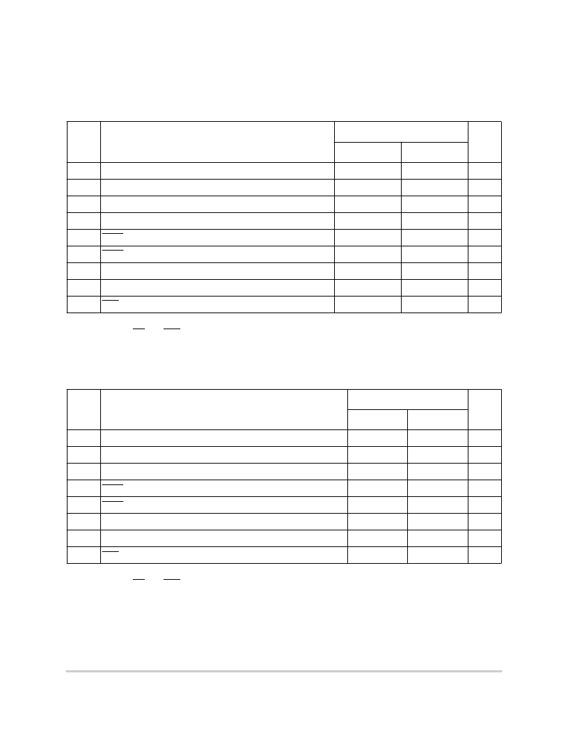
Table 11-18. NMSI External Clock Timing
Num
Characteristic
All Frequencies
Unit
Min
Max
100
RCLK1 and TCLK1 width high
1
1
The ratios SYNCCLK/RCLK1 and SYNCCLK/TCLK1 must be greater than or equal to 2.25/1.
2
Also applies to CD and CTS hold time when they are used as an external sync signal.
1/SYNCCLK
—
ns
101
RCLK1 and TCLK1 width low
1/SYNCCLK + 5
—
ns
102
RCLK1 and TCLK1 rise/fall time
—
15.00
ns
103
TXD1 active delay (from TCLK1 falling edge)
0.00
50.00
ns
104
RTS1 active/inactive delay (from TCLK1 falling edge)
0.00
50.00
ns
105
CTS1 setup time to TCLK1 rising edge
5.00
—
ns
106
RXD1 setup time to RCLK1 rising edge
5.00
—
ns
107
RXD1 hold time from RCLK1 rising edge
2
5.00
—
ns
108
CD1 setup Time to RCLK1 rising edge
5.00
—
ns
Table 11-19. NMSI Internal Clock Timing
Num
Characteristic
All Frequencies
Unit
Min
Max
100
RCLK1 and TCLK1 frequency
1
1
The ratios SYNCCLK/RCLK1 and SYNCCLK/TCLK1 must be greater or equal to 3/1.
2
Also applies to CD and CTS hold time when they are used as an external sync signals.
0.00
SYNCCLK/3
MHz
102
RCLK1 and TCLK1 rise/fall time
—
—
ns
103
TXD1 active delay (from TCLK1 falling edge)
0.00
30.00
ns
104
RTS1 active/inactive delay (from TCLK1 falling edge)
0.00
30.00
ns
105
CTS1 setup time to TCLK1 rising edge
40.00
—
ns
106
RXD1 setup time to RCLK1 rising edge
40.00
—
ns
107
RXD1 hold time from RCLK1 rising edge
2
0.00
—
ns
108
CD1 setup time to RCLK1 rising edge
40.00
—
ns
相關(guān)PDF資料 |
PDF描述 |
|---|---|
| XPC855TZP66D4 | Family Hardware Specifications |
| XPC860DECZP66D4 | Family Hardware Specifications |
| XPC860DEZP66D4 | Family Hardware Specifications |
| XPC860DPCZP50D4 | Family Hardware Specifications |
| XPC860DPCZP66D3 | Family Hardware Specifications |
相關(guān)代理商/技術(shù)參數(shù) |
參數(shù)描述 |
|---|---|
| XPC860ZP25 | 制造商:未知廠家 制造商全稱:未知廠家 功能描述:Communications Controller |
| XPC860ZP33C1 | 制造商:Rochester Electronics LLC 功能描述:- Bulk 制造商:Motorola Inc 功能描述: 制造商:MOTOROLA 功能描述: |
| XPC860ZP40 | 制造商:未知廠家 制造商全稱:未知廠家 功能描述:Communications Controller |
| XPC860ZP50C1 | 制造商:FRESCL 功能描述: 制造商:Motorola Inc 功能描述: |
| XPC860ZP66C1 | 制造商:未知廠家 制造商全稱:未知廠家 功能描述:COMMUNICATIONS CONTROLLER |
發(fā)布緊急采購,3分鐘左右您將得到回復(fù)。