- 您現(xiàn)在的位置:買(mǎi)賣(mài)IC網(wǎng) > PDF目錄3980 > XC4028XLA-09HQ240I (Xilinx Inc)IC FPGA I 2.5V 256 I/O 240HQFP PDF資料下載
參數(shù)資料
| 型號(hào): | XC4028XLA-09HQ240I |
| 廠商: | Xilinx Inc |
| 文件頁(yè)數(shù): | 9/14頁(yè) |
| 文件大小: | 0K |
| 描述: | IC FPGA I 2.5V 256 I/O 240HQFP |
| 產(chǎn)品變化通告: | XC1700 PROMs,XC5200,HQ,SCD Parts Discontinuation 19/Jul/2010 |
| 標(biāo)準(zhǔn)包裝: | 24 |
| 系列: | XC4000XLA/XV |
| LAB/CLB數(shù): | 1024 |
| 邏輯元件/單元數(shù): | 2432 |
| RAM 位總計(jì): | 32768 |
| 輸入/輸出數(shù): | 193 |
| 門(mén)數(shù): | 28000 |
| 電源電壓: | 3 V ~ 3.6 V |
| 安裝類(lèi)型: | 表面貼裝 |
| 工作溫度: | -40°C ~ 100°C |
| 封裝/外殼: | 240-BFQFP 裸露焊盤(pán) |
| 供應(yīng)商設(shè)備封裝: | 240-PQFP(32x32) |
| 其它名稱(chēng): | Q1143124 XC4028XLA09HQ240I |
第1頁(yè)第2頁(yè)第3頁(yè)第4頁(yè)第5頁(yè)第6頁(yè)第7頁(yè)第8頁(yè)當(dāng)前第9頁(yè)第10頁(yè)第11頁(yè)第12頁(yè)第13頁(yè)第14頁(yè)

R
XC4000XLA/XV Field Programmable Gate Arrays
6-160
DS015 (v2.0) March 1, 2013 - Product Specification
Product Obsolete/Under Obsolescence
Using Fast I/O CLKS
There are several issues associated with implementing fast
I/O clocks by using multiple FastCLK and BUFGE clock buf-
fers for I/O transfers and a BUFGLS clock buffer for internal
logic.
Reduced Clock to Out Period - When transferring data
from a BUFGLS clocked register to an IOB output register
which is clocked with a fast I/O clock, the total amount of
time available for the transfer is reduced.
Using Fast Capture Latch in IOB input - It is necessary to
transfer data captured with the fast I/O clock edge to a
delayed BUFGLS clock without error. The use of the Fast
Capture Latch in the IOBs provides this functionality.
Driving multiple clock inputs - Since each FastCLK input
can only reach one octant of IOBs it will usually be neces-
sary to drive multiple FastCLK and BUFGE input pads with
a copy of the system clock. Xilinx recommends that sys-
tems which use multiple FastCLK and BUFGE input buffers
use a “Zero Delay” clock buffer such as the Cypress
CY2308 to drive up to 8 input pins. These devices contain a
Phase locked loop to eliminate clock delay, and specify less
than 250ps output jitter.
PCB layout - The recommended layout is to place the PLL
underneath the FPGA on the reverse side of the PCB. All 8
clock lines should be of equal length. This arrangement will
allow all the clock line to be less than 2 cm in length which
will generally eliminate the need for clock termination.
Advancing the FPGAs clock - An additional advantage to
using a PLL-equipped clock buffer is that it can advance the
FPGA clocks relative to the system clock by incorporating
additional board delay in the feedback path. Approximately
6 inches of trace length are necessary to delay the signal
by 1 ns.
Advancing the FPGA’s clock directly reduces input hold
requirements and improves clock to out delay. FPGA clocks
should not be advanced more than the guaranteed mini-
mum Output Hold Time (minus any associated clock jitter)
or the outputs may change state before the system clock
edge. For XLA and XV FPGAs the Output Hold Time is
specified as a minimum Clock to Output Delay in the tables
in the respective family Electrical Specification sections.
The maximum recommended clock advance equals this
value minus any clock jitter.
Instantiating I/O elements- Depending on the design
environment, it may be necessary to instantiate the fast I/O
elements. They are found in the libraries as:
BUFGE (I,O) - The Global Early Buffer
BUFGLS (I,O)- The Global Low Skew Buffer
BUFFCLK (I,O) - The FastCLK Buffer
ILFFX (D, GF, CE, C, Q) - The Fast Capture Latch
Macro
Locating I/O elements - It is necessary to connect these
elements to a particular I/O pad in order to select which buf-
fer or fast capture latch will be used.
Restricted Clock Loading - Because the input hold
requirement is a function of internal clock delay, it may be
necessary to restrict the routing of BUFGE to IOBs along
the top and bottom of the die to obtain sub-ns clock delays.
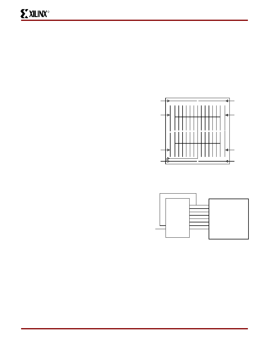
BUFGE 1
BUFGE 2
FCLK 3
FCLK 4
BUFGE 5
FCLK 2
FCLK 1
BUFGE 6
BUFGLS 2
Figure 2: Location of FastCLK, BUFGE and BUFGLS
Clock Buffers in XC4000XLA/XV FPGAs
BUFGE
1
BUFGE
2
BUFGE
5
BUFGE
6
FCLK1
FCLK2
FCLK3
FCLK4
PLL
Clock
Buffer
O0
O1
O2
O3
O4
O5
O6
O7
FB
Ref
XC4000XLA
XC4000XV
SysClk
Figure 3: Diagram of XC4000XLA/XV FPGA
Connected to PLL Clock Buffer Driving 4 BUFGE and
4 FastCLK Clock Buffers.
相關(guān)PDF資料 |
PDF描述 |
|---|---|
| IDT70V3579S5BF | IC SRAM 1.125MBIT 5NS 208FBGA |
| HMM44DREH | CONN EDGECARD 88POS .156 EYELET |
| KMPC885ZP133 | IC MPU POWERQUICC 133MHZ 357PBGA |
| IDT70V3389S5BF | IC SRAM 1.125MBIT 5NS 208FBGA |
| ASM43DREI | CONN EDGECARD 86POS .156 EYELET |
相關(guān)代理商/技術(shù)參數(shù) |
參數(shù)描述 |
|---|---|
| XC4028XLT-09HQ240C | 制造商:Xilinx 功能描述: |
| XC4028XLT-1HQ240C | 制造商:Xilinx 功能描述: |
| XC4036EX-2BG432C | 制造商:Xilinx 功能描述: |
| XC4036EX-2HQ240C | 制造商:Xilinx 功能描述: |
| XC4036EX-3BG352I | 制造商:Xilinx 功能描述: |
發(fā)布緊急采購(gòu),3分鐘左右您將得到回復(fù)。