- 您現(xiàn)在的位置:買賣IC網(wǎng) > PDF目錄4294 > XC3S250E-5VQG100C (Xilinx Inc)IC FPGA SPARTAN-3E 250K 100-VQFP PDF資料下載
參數(shù)資料
| 型號(hào): | XC3S250E-5VQG100C |
| 廠商: | Xilinx Inc |
| 文件頁數(shù): | 20/227頁 |
| 文件大小: | 0K |
| 描述: | IC FPGA SPARTAN-3E 250K 100-VQFP |
| 標(biāo)準(zhǔn)包裝: | 90 |
| 系列: | Spartan®-3E |
| LAB/CLB數(shù): | 612 |
| 邏輯元件/單元數(shù): | 5508 |
| RAM 位總計(jì): | 221184 |
| 輸入/輸出數(shù): | 66 |
| 門數(shù): | 250000 |
| 電源電壓: | 1.14 V ~ 1.26 V |
| 安裝類型: | 表面貼裝 |
| 工作溫度: | 0°C ~ 85°C |
| 封裝/外殼: | 100-TQFP |
| 供應(yīng)商設(shè)備封裝: | 100-VQFP(14x14) |
第1頁第2頁第3頁第4頁第5頁第6頁第7頁第8頁第9頁第10頁第11頁第12頁第13頁第14頁第15頁第16頁第17頁第18頁第19頁當(dāng)前第20頁第21頁第22頁第23頁第24頁第25頁第26頁第27頁第28頁第29頁第30頁第31頁第32頁第33頁第34頁第35頁第36頁第37頁第38頁第39頁第40頁第41頁第42頁第43頁第44頁第45頁第46頁第47頁第48頁第49頁第50頁第51頁第52頁第53頁第54頁第55頁第56頁第57頁第58頁第59頁第60頁第61頁第62頁第63頁第64頁第65頁第66頁第67頁第68頁第69頁第70頁第71頁第72頁第73頁第74頁第75頁第76頁第77頁第78頁第79頁第80頁第81頁第82頁第83頁第84頁第85頁第86頁第87頁第88頁第89頁第90頁第91頁第92頁第93頁第94頁第95頁第96頁第97頁第98頁第99頁第100頁第101頁第102頁第103頁第104頁第105頁第106頁第107頁第108頁第109頁第110頁第111頁第112頁第113頁第114頁第115頁第116頁第117頁第118頁第119頁第120頁第121頁第122頁第123頁第124頁第125頁第126頁第127頁第128頁第129頁第130頁第131頁第132頁第133頁第134頁第135頁第136頁第137頁第138頁第139頁第140頁第141頁第142頁第143頁第144頁第145頁第146頁第147頁第148頁第149頁第150頁第151頁第152頁第153頁第154頁第155頁第156頁第157頁第158頁第159頁第160頁第161頁第162頁第163頁第164頁第165頁第166頁第167頁第168頁第169頁第170頁第171頁第172頁第173頁第174頁第175頁第176頁第177頁第178頁第179頁第180頁第181頁第182頁第183頁第184頁第185頁第186頁第187頁第188頁第189頁第190頁第191頁第192頁第193頁第194頁第195頁第196頁第197頁第198頁第199頁第200頁第201頁第202頁第203頁第204頁第205頁第206頁第207頁第208頁第209頁第210頁第211頁第212頁第213頁第214頁第215頁第216頁第217頁第218頁第219頁第220頁第221頁第222頁第223頁第224頁第225頁第226頁第227頁
Spartan-3E FPGA Family: DC and Switching Characteristics
DS312 (v4.1) July 19, 2013
Product Specification
116
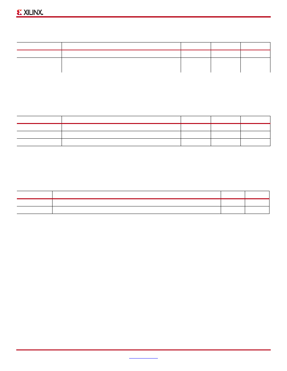
Power Supply Specifications
Table 74: Supply Voltage Thresholds for Power-On Reset
Symbol
Description
Min
Max
Units
VCCINTT
Threshold for the VCCINT supply
0.4
1.0
V
VCCAUXT
Threshold for the VCCAUX supply
0.8
2.0
V
VCCO2T
Threshold for the VCCO Bank 2 supply
0.4
1.0
V
Notes:
1.
VCCINT, VCCAUX, and VCCO supplies to the FPGA can be applied in any order. However, the FPGA’s configuration source (Platform Flash,
SPI Flash, parallel NOR Flash, microcontroller) might have specific requirements. Check the data sheet for the attached configuration
source. In Step 0 devices using the HSWAP internal pull-up, VCCINT must be applied before VCCAUX.
2.
To ensure successful power-on, VCCINT, VCCO Bank 2, and VCCAUX supplies must rise through their respective threshold-voltage ranges with
no dips at any point.
Table 75: Supply Voltage Ramp Rate
Symbol
Description
Min
Max
Units
VCCINTR
Ramp rate from GND to valid VCCINT supply level
0.2
50
ms
VCCAUXR
Ramp rate from GND to valid VCCAUX supply level
0.2
50
ms
VCCO2R
Ramp rate from GND to valid VCCO Bank 2 supply level
0.2
50
ms
Notes:
1.
VCCINT, VCCAUX, and VCCO supplies to the FPGA can be applied in any order. However, the FPGA’s configuration source (Platform Flash,
SPI Flash, parallel NOR Flash, microcontroller) might have specific requirements. Check the data sheet for the attached configuration
source. In Step 0 devices using the HSWAP internal pull-up, VCCINT must be applied before VCCAUX.
2.
To ensure successful power-on, VCCINT, VCCO Bank 2, and VCCAUX supplies must rise through their respective threshold-voltage ranges with
no dips at any point.
Table 76: Supply Voltage Levels Necessary for Preserving RAM Contents
Symbol
Description
Min
Units
VDRINT
VCCINT level required to retain RAM data
1.0
V
VDRAUX
VCCAUX level required to retain RAM data
2.0
V
Notes:
1.
RAM contents include configuration data.
相關(guān)PDF資料 |
PDF描述 |
|---|---|
| 93C66A-E/P | IC EEPROM 4KBIT 2MHZ 8DIP |
| 24LCS52-I/P | IC EEPROM 2KBIT 400KHZ 8DIP |
| 24LCS21A/SN | IC EEPROM 1KBIT 400KHZ 8SOIC |
| 24LCS21AT/SN | IC EEPROM 1KBIT 400KHZ 8SOIC |
| 24LCS21AT-I/SN | IC EEPROM 1KBIT 400KHZ 8SOIC |
相關(guān)代理商/技術(shù)參數(shù) |
參數(shù)描述 |
|---|---|
| XC3S250E-5VQG100I | 制造商:XILINX 制造商全稱:XILINX 功能描述:Spartan-3E FPGA Family |
| XC3S400 | 制造商:XILINX 制造商全稱:XILINX 功能描述:XC17V00 Series Configuration PROMs |
| XC3S4000 | 制造商:XILINX 制造商全稱:XILINX 功能描述:Spartan-3 FPGA |
| XC3S4000-4CP132C | 制造商:XILINX 制造商全稱:XILINX 功能描述:Spartan-3 FPGA |
| XC3S4000-4CP132I | 制造商:XILINX 制造商全稱:XILINX 功能描述:Spartan-3 FPGA |
發(fā)布緊急采購(gòu),3分鐘左右您將得到回復(fù)。