- 您現(xiàn)在的位置:買賣IC網(wǎng) > PDF目錄4294 > XC3S250E-5VQG100C (Xilinx Inc)IC FPGA SPARTAN-3E 250K 100-VQFP PDF資料下載
參數(shù)資料
| 型號: | XC3S250E-5VQG100C |
| 廠商: | Xilinx Inc |
| 文件頁數(shù): | 183/227頁 |
| 文件大小: | 0K |
| 描述: | IC FPGA SPARTAN-3E 250K 100-VQFP |
| 標準包裝: | 90 |
| 系列: | Spartan®-3E |
| LAB/CLB數(shù): | 612 |
| 邏輯元件/單元數(shù): | 5508 |
| RAM 位總計: | 221184 |
| 輸入/輸出數(shù): | 66 |
| 門數(shù): | 250000 |
| 電源電壓: | 1.14 V ~ 1.26 V |
| 安裝類型: | 表面貼裝 |
| 工作溫度: | 0°C ~ 85°C |
| 封裝/外殼: | 100-TQFP |
| 供應商設備封裝: | 100-VQFP(14x14) |
第1頁第2頁第3頁第4頁第5頁第6頁第7頁第8頁第9頁第10頁第11頁第12頁第13頁第14頁第15頁第16頁第17頁第18頁第19頁第20頁第21頁第22頁第23頁第24頁第25頁第26頁第27頁第28頁第29頁第30頁第31頁第32頁第33頁第34頁第35頁第36頁第37頁第38頁第39頁第40頁第41頁第42頁第43頁第44頁第45頁第46頁第47頁第48頁第49頁第50頁第51頁第52頁第53頁第54頁第55頁第56頁第57頁第58頁第59頁第60頁第61頁第62頁第63頁第64頁第65頁第66頁第67頁第68頁第69頁第70頁第71頁第72頁第73頁第74頁第75頁第76頁第77頁第78頁第79頁第80頁第81頁第82頁第83頁第84頁第85頁第86頁第87頁第88頁第89頁第90頁第91頁第92頁第93頁第94頁第95頁第96頁第97頁第98頁第99頁第100頁第101頁第102頁第103頁第104頁第105頁第106頁第107頁第108頁第109頁第110頁第111頁第112頁第113頁第114頁第115頁第116頁第117頁第118頁第119頁第120頁第121頁第122頁第123頁第124頁第125頁第126頁第127頁第128頁第129頁第130頁第131頁第132頁第133頁第134頁第135頁第136頁第137頁第138頁第139頁第140頁第141頁第142頁第143頁第144頁第145頁第146頁第147頁第148頁第149頁第150頁第151頁第152頁第153頁第154頁第155頁第156頁第157頁第158頁第159頁第160頁第161頁第162頁第163頁第164頁第165頁第166頁第167頁第168頁第169頁第170頁第171頁第172頁第173頁第174頁第175頁第176頁第177頁第178頁第179頁第180頁第181頁第182頁當前第183頁第184頁第185頁第186頁第187頁第188頁第189頁第190頁第191頁第192頁第193頁第194頁第195頁第196頁第197頁第198頁第199頁第200頁第201頁第202頁第203頁第204頁第205頁第206頁第207頁第208頁第209頁第210頁第211頁第212頁第213頁第214頁第215頁第216頁第217頁第218頁第219頁第220頁第221頁第222頁第223頁第224頁第225頁第226頁第227頁
Spartan-3E FPGA Family: Functional Description
DS312 (v4.1) July 19, 2013
Product Specification
59
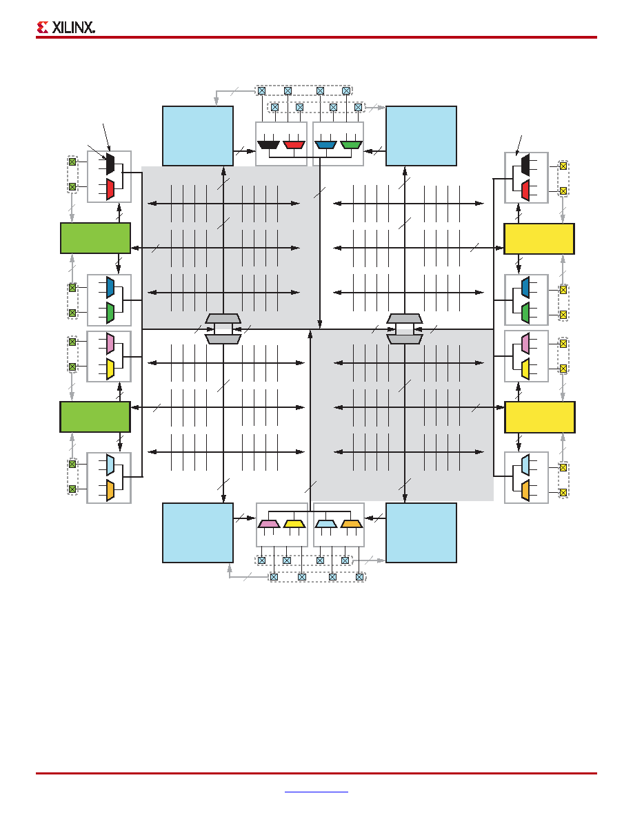
X-Ref Target - Figure 45
Figure 45: Spartan-3E Internal Quadrant-Based Clock Network (Electrical Connectivity View)
8
88
4
8
Left Spine
Top Left
Quadrant (TL)
Top Right
Quadrant (TR)
Bottom Right
Quadrant (BR)
Bottom Left
Quadrant (BL)
Right Spine
Horizontal
Spine
T
op
S
pine
Bottom
S
pine
4
DS312-2_04_041106
DCM
XC3S250E (X0Y1)
XC3S500E (X0Y1)
XC3S1200E (X1Y3)
XC3S1600E (X1Y3)
4
DCM
XC3S250E (X0Y0)
XC3S500E (X0Y0)
XC3S1200E (X1Y0)
XC3S1600E (X1Y0)
4
DCM
XC3S100E (X0Y1)
XC3S250E (X1Y1)
XC3S500E (X1Y1)
XC3S1200E (X2Y3)
XC3S1600E (X2Y3)
4
DCM
XC3S100E (X0Y0)
XC3S250E (X1Y0)
XC3S500E (X1Y0)
XC3S1200E (X2Y0)
XC3S1600E (X2Y0)
X1Y10 X1Y11
X2Y10 X2Y11
GCLK6
GCLK7
GCLK10
GCLK11
GCLK4
GCLK5
GCLK8
GCLK9
X1Y0 X1Y1
X2Y0 X2Y1
GCLK14
GCLK15
GCLK2
GCLK3
GCLK12
GCLK13
GCLK0
GCLK1
X0Y6
X0Y7
X0Y
8
X0Y9
LHCLK5
LHCLK4
LHCLK7
LHCLK6
X0Y2
X0Y
3
X0Y4
X0Y5
LHCLK1
LHCLK0
LHCLK
3
LHCLK2
X
3
Y5
X
3
Y4
X
3
Y
3
X
3
Y2
RHCLK6
RHCLK7
RHCLK4
RHCLK5
X
3
Y9
X
3
Y
8
X
3
Y7
X
3
Y6
RHCLK2
RHCLK
3
RHCLK0
RHCLK1
2
DCM
XC3S1200E (X0Y1)
XC3S1600E (X0Y1)
2
DCM
XC3S1200E (X0Y2)
XC3S1600E (X0Y2)
DCM
XC3S1200E (X3Y2)
XC3S1600E (X3Y2)
DCM
XC3S1200E (X3Y1)
XC3S1600E (X3Y1)
Global Clock Inputs
Left-Half
Cloc
k
Input
s
Ri
g
ht-Half
Cloc
k
Input
s
BUFGMUX
H
G
B
A
D
C
F
E
A
C
H
G
B
A
D
C
F
E
B
D
E
GF
H
pair
Clock Line
in Quadrant
Note 4
Note 3
8
4
8
2
Notes:
1.
The diagram presents electrical connectivity. The diagram locations do not necessarily match the physical location on the
device, although the coordinate locations shown are correct.
2.
Number of DCMs and locations of these DCM varies for different device densities. The left and right DCMs are only in the
XC3S1200E and XC3S1600E. The XC3S100E has only two DCMs, one on the top right and one on the bottom right of the die.
3.
See Figure 47a, which shows how the eight clock lines are multiplexed on the left-hand side of the device.
4.
See Figure 47b, which shows how the eight clock lines are multiplexed on the right-hand side of the device.
5.
For best direct clock inputs to a particular clock buffer, not a DCM, see Table 41.
6.
For best direct clock inputs to a particular DCM, not a BUFGMUX, see Table 30, Table 31, and Table 32. Direct pin inputs to a
DCM are shown in gray.
相關PDF資料 |
PDF描述 |
|---|---|
| 93C66A-E/P | IC EEPROM 4KBIT 2MHZ 8DIP |
| 24LCS52-I/P | IC EEPROM 2KBIT 400KHZ 8DIP |
| 24LCS21A/SN | IC EEPROM 1KBIT 400KHZ 8SOIC |
| 24LCS21AT/SN | IC EEPROM 1KBIT 400KHZ 8SOIC |
| 24LCS21AT-I/SN | IC EEPROM 1KBIT 400KHZ 8SOIC |
相關代理商/技術參數(shù) |
參數(shù)描述 |
|---|---|
| XC3S250E-5VQG100I | 制造商:XILINX 制造商全稱:XILINX 功能描述:Spartan-3E FPGA Family |
| XC3S400 | 制造商:XILINX 制造商全稱:XILINX 功能描述:XC17V00 Series Configuration PROMs |
| XC3S4000 | 制造商:XILINX 制造商全稱:XILINX 功能描述:Spartan-3 FPGA |
| XC3S4000-4CP132C | 制造商:XILINX 制造商全稱:XILINX 功能描述:Spartan-3 FPGA |
| XC3S4000-4CP132I | 制造商:XILINX 制造商全稱:XILINX 功能描述:Spartan-3 FPGA |
發(fā)布緊急采購,3分鐘左右您將得到回復。