- 您現(xiàn)在的位置:買賣IC網(wǎng) > PDF目錄359452 > VV5410 (意法半導(dǎo)體) Mono and Colour Digital Video CMOS Image Sensors PDF資料下載
參數(shù)資料
| 型號: | VV5410 |
| 廠商: | 意法半導(dǎo)體 |
| 英文描述: | Mono and Colour Digital Video CMOS Image Sensors |
| 中文描述: | 莫諾和數(shù)字視頻彩色CMOS圖像傳感器 |
| 文件頁數(shù): | 10/105頁 |
| 文件大?。?/td> | 489K |
| 代理商: | VV5410 |
第1頁第2頁第3頁第4頁第5頁第6頁第7頁第8頁第9頁當(dāng)前第10頁第11頁第12頁第13頁第14頁第15頁第16頁第17頁第18頁第19頁第20頁第21頁第22頁第23頁第24頁第25頁第26頁第27頁第28頁第29頁第30頁第31頁第32頁第33頁第34頁第35頁第36頁第37頁第38頁第39頁第40頁第41頁第42頁第43頁第44頁第45頁第46頁第47頁第48頁第49頁第50頁第51頁第52頁第53頁第54頁第55頁第56頁第57頁第58頁第59頁第60頁第61頁第62頁第63頁第64頁第65頁第66頁第67頁第68頁第69頁第70頁第71頁第72頁第73頁第74頁第75頁第76頁第77頁第78頁第79頁第80頁第81頁第82頁第83頁第84頁第85頁第86頁第87頁第88頁第89頁第90頁第91頁第92頁第93頁第94頁第95頁第96頁第97頁第98頁第99頁第100頁第101頁第102頁第103頁第104頁第105頁
VV5410 & VV6410
Operating Modes
cd5410-6410f-3-0.fm
Commercial in confidence
10/105
note1: The free running qck, slow by default, is enabled by writing 8’h04 to serial register [20].
note2: The contents of the extra black lines are enabled on to the data bus by setting bit [5] of serial register [17]. If bit [0] of serial
register [24] is reset, indicating that the preferred coprocessor device is not the VP3 device, (a STMicroelectronics coprocessor),
then the extra black lines are enabled by default regardless of the basic video mode selected.
The registers that control the image position within the pixel array and also the order in which the pixels are read out have not
been included in the table as their values are subject to a secondary series of registers. We will discuss the former in sections 2.2
and 2.3.
3.1.2
It is recommended that a 16 MHz clock is used to generate CIF-25fps,CIF-30fps and QCIF-60fps and that an 8 MHz clock is used
to generate QCIF-25fps and QCIF-30fps, however the sensor can adapt to a range of other input frequencies and still generate
the required frame rates. For example, a 24 MHz clock can be used to generate CIF-30fps. By setting bit [7] of serial register [22]
the sensor can automatically divide the incoming clock by 1.5 by setting bit [7] of serial register [22], such that the internal clock
generator logic will still receive a 16 MHz clock.
Input Clock Frequencies
Note that the clock division register is internally an 8 bit value, although the user may only program the lower nibble. The upper
nibble is reserved for setting the clock divisor as we change between primary video modes. The lower nibble can be programmed
to reduce the effective frame rate within each video mode.
The system clock divisor column in Table 5 assumes that the programmable pixel clock divisor is set to the default of 0,
implementing a divide by 1 of the internal pixel clock. Consider the following scenario where a user requires 15 fps CIF resolution
image. As can be seen there are a wide range of options to achieve the same result.
3.2
The physical pixel array is 364 x 296 pixels. The pixel size is 7.5
μ
m by 6.9
μ
m. The image size for NTSC is 306 x 244 pixels, for
PAL and CIF it is 356 x 292 pixels, while for the QCIF modes the image size is 180 x 148 pixels. The remaining 4 physical
columns on each side of the PAL image size prevent columns 1 and 2 in PAL/CIF modes from being distorted by the edge effects
which occur when a pixel is close to the outer edge of the physical pixel array. Please note that these columns can be enabled as
part of the visible image if the user is operating the sensor in the pantilt QCIF mode.
Pixel Array
Figure 3 shows how the 306 x 244 and 180 x 148 sub-arrays are aligned within the bigger 364 x 296 pixel array. The Bayer
colourisation pattern requires that the top-left corner of the pixel sub-array is always a Green 1 pixel. To preserve this Bayer
colour pattern the NTSC sub-array has been offset relative to the centre of the array. The QCIF size images are centrally
orientated.
Image read-out is very flexible. Sections 3.3.2 - describe the options available to the user. By default the sensor read out is
configured to be horizontally ‘shuffled’ non-interlaced raster scan. The horizontally ‘shuffled’ raster scan order differs from a
conventional raster in that the pixels of individual rows are re-ordered, with the odd pixels within a row read-out first, followed by
the even pixels. This ‘shuffled’ read-out within a line, groups pixels of the same colour (according to the Bayer pattern - Figure 2)
together, reducing cross talk between the colour channels. This option is on by default and is controllable via the serial interface.
The horizontal shuffle option would normally only be selected with the colour sensor variant, VV6410.
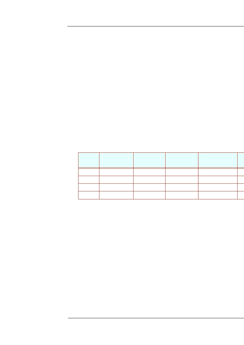
clk in
(MHz)
Divide by 3/2
enabled
Systemclock
divisor
Pixel clock
divisor
pclk (MHz)
Field Rate
8
no
4
1
2
15
12
yes
4
1
2
15
16
no
4
2
2
15
24
yes
4
2
2
15
Table 5 : System clock divisor options
相關(guān)PDF資料 |
PDF描述 |
|---|---|
| VV5430C001 | Monochrome Analog Output CMOS Image Sensors |
| VV5430 | Integrated CMOS Image Sensor with support for ADC and external control via serial interface |
| VV6410C036 | DUAL-MODE DIGITAL CAMERA CHIPSET |
| VV6410 | XTAL MTL T/H HC49/US |
| VV6444 | Low Cost Digital Camera (LCDC) Chipset |
相關(guān)代理商/技術(shù)參數(shù) |
參數(shù)描述 |
|---|---|
| VV5410C036 | 制造商:STMicroelectronics 功能描述:IMAGE SENSOR MONOCHROME CMOS 352X288PIXELS 36CLCC - Bulk |
| VV5430 | 制造商:未知廠家 制造商全稱:未知廠家 功能描述:Integrated CMOS Image Sensor with support for ADC and external control via serial interface |
| VV5430C001 | 制造商:STMICROELECTRONICS 制造商全稱:STMicroelectronics 功能描述:Monochrome Analog Output CMOS Image Sensors |
| VV5501C001 | 功能描述:視頻 IC Monochrome Sensor RoHS:否 制造商:Fairchild Semiconductor 工作電源電壓:5 V 電源電流:80 mA 最大工作溫度:+ 85 C 封裝 / 箱體:TSSOP-28 封裝:Reel |
| VV5F3-30-041 | 制造商:SMC Corporation of America 功能描述:Manifold Base for VF series, base mt, 1/4 inch |
發(fā)布緊急采購,3分鐘左右您將得到回復(fù)。