- 您現(xiàn)在的位置:買賣IC網(wǎng) > PDF目錄359352 > VCT3801A (MICRONAS SEMICONDUCTOR HOLDING AG) Video/Controller/Teletext IC Family PDF資料下載
參數(shù)資料
| 型號(hào): | VCT3801A |
| 廠商: | MICRONAS SEMICONDUCTOR HOLDING AG |
| 英文描述: | Video/Controller/Teletext IC Family |
| 中文描述: | 視頻/控制/圖文電視IC系列 |
| 文件頁數(shù): | 107/172頁 |
| 文件大?。?/td> | 2243K |
| 代理商: | VCT3801A |
第1頁第2頁第3頁第4頁第5頁第6頁第7頁第8頁第9頁第10頁第11頁第12頁第13頁第14頁第15頁第16頁第17頁第18頁第19頁第20頁第21頁第22頁第23頁第24頁第25頁第26頁第27頁第28頁第29頁第30頁第31頁第32頁第33頁第34頁第35頁第36頁第37頁第38頁第39頁第40頁第41頁第42頁第43頁第44頁第45頁第46頁第47頁第48頁第49頁第50頁第51頁第52頁第53頁第54頁第55頁第56頁第57頁第58頁第59頁第60頁第61頁第62頁第63頁第64頁第65頁第66頁第67頁第68頁第69頁第70頁第71頁第72頁第73頁第74頁第75頁第76頁第77頁第78頁第79頁第80頁第81頁第82頁第83頁第84頁第85頁第86頁第87頁第88頁第89頁第90頁第91頁第92頁第93頁第94頁第95頁第96頁第97頁第98頁第99頁第100頁第101頁第102頁第103頁第104頁第105頁第106頁當(dāng)前第107頁第108頁第109頁第110頁第111頁第112頁第113頁第114頁第115頁第116頁第117頁第118頁第119頁第120頁第121頁第122頁第123頁第124頁第125頁第126頁第127頁第128頁第129頁第130頁第131頁第132頁第133頁第134頁第135頁第136頁第137頁第138頁第139頁第140頁第141頁第142頁第143頁第144頁第145頁第146頁第147頁第148頁第149頁第150頁第151頁第152頁第153頁第154頁第155頁第156頁第157頁第158頁第159頁第160頁第161頁第162頁第163頁第164頁第165頁第166頁第167頁第168頁第169頁第170頁第171頁第172頁
ADVANCE INFORMATION
VCT 38xxA
Micronas
107
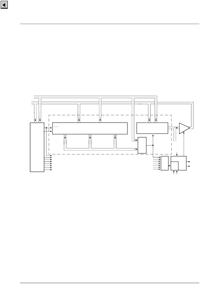
5.11.Memory Patch Module
The Memory Patch Module allows the user to modify
up to ten hard-wired ROM locations by external
means. This function is useful if faulty parts of software
or data are detected after the ROM code has been
cast into mask ROM.
Software loads addresses and the corrected code e.g.
from external non-volatile memory into respective
registers of the module. The module then will replace
faulty code upon address match.
Single ROM locations are directly replaced. Longer
faulty sequences may be repaired by introducing a
jump to a new subroutine in RAM (e.g. opcode JSR
requires 3 consecutive bytes to be patched). The RAM
subroutine then may consist of any number of instruc-
tions, ending with a return to the next correct instruc-
tion in ROM. In such a way it is possible to include also
complex software modules.
5.11.1.Features
– patching of read data from up to 10 different ROM
locations (24 bit physical address)
– automatic insertion of 1 CPU wait state for each
patched access
Fig. 5–16:
Block diagram of patch module
5.11.2.General
The logic contains ten patch cells (see Fig. 5–16 on
page 107), each consisting of a 24-bit compare regis-
ter (Patch Address register, PARn), a 24-bit address
comparator, a Patch Enable register (PERn) bit and an
8-bit Patch Data register (PDR).
The current address information for a ROM access is
fed to a bank of ten patch cells. In case of a match in
one patch cell, and provided that the corresponding
Patch Enable register bit is set, a wait cycle for CPU is
included by pulling down the RDY input of CPU for one
cycle (see Fig. on page 108). In the meantime the
module’s logic disables the ROM data bus drivers and
instead places the data information from the corre-
sponding Patch Data register on the data bus.
5.11.3.Initialization
After reset, as bit PER0.PMEN is reset to 0, all patch
cell registers are in Write mode and patch operation is
disabled.
To initialize a patch cell, first set the corresponding
PSEL bit in register PER0 or PER1 as a pointer. Then
enter the 24bit address to registers PAR2 (High byte),
PAR1 (middle byte) and PAR0 (Low byte) and the
desired patch code to register PDR.
If desired, repeat the above sequence for other patch
cells. Only set one PSEL pointer bit in registers PER0
and PER1 at a time.
PA[23:16]
PA[7:0]
ADB[23:0]
DB[7:0]
≥
1
PA[15:8]
Patch Address Register
P
Output Enable
Patch Data
Patch Cell 0
Patch Cells 1...9
Register
Enable
Write/Compare
Sequencer
P
P
DBP[7:0]
RDY
ROMEN
RWQ
ROMACC
PH2
PATOE
&
≡
相關(guān)PDF資料 |
PDF描述 |
|---|---|
| VCU2133 | High-Speed coder/decoder IC |
| VCX2150A | Surface mount 15.88 mm SQ (.625 SQ) |
| VCX2154A | Surface mount 15.88 mm SQ (.625 SQ) |
| VCXO-105N | VCXO |
| VCXO-199 | VCXO |
相關(guān)代理商/技術(shù)參數(shù) |
參數(shù)描述 |
|---|---|
| VCT3802A | 制造商:MICRONAS 制造商全稱:MICRONAS 功能描述:Video/Controller/Teletext IC Family |
| VCT3803A | 制造商:MICRONAS 制造商全稱:MICRONAS 功能描述:Video/Controller/Teletext IC Family |
| VCT3804A | 制造商:MICRONAS 制造商全稱:MICRONAS 功能描述:Video/Controller/Teletext IC Family |
| VCT3811A | 制造商:MICRONAS 制造商全稱:MICRONAS 功能描述:Video/Controller/Teletext IC Family |
| VCT3831A | 制造商:MICRONAS 制造商全稱:MICRONAS 功能描述:Video/Controller/Teletext IC Family |
發(fā)布緊急采購,3分鐘左右您將得到回復(fù)。