- 您現(xiàn)在的位置:買賣IC網(wǎng) > PDF目錄383986 > USB97C243 (SMSC Corporation) capacitor Selection for Internal Regulator Output Pins PDF資料下載
參數(shù)資料
| 型號: | USB97C243 |
| 廠商: | SMSC Corporation |
| 英文描述: | capacitor Selection for Internal Regulator Output Pins |
| 中文描述: | 電容的選擇內(nèi)部穩(wěn)壓器輸出引腳 |
| 文件頁數(shù): | 54/59頁 |
| 文件大小: | 385K |
| 代理商: | USB97C243 |
第1頁第2頁第3頁第4頁第5頁第6頁第7頁第8頁第9頁第10頁第11頁第12頁第13頁第14頁第15頁第16頁第17頁第18頁第19頁第20頁第21頁第22頁第23頁第24頁第25頁第26頁第27頁第28頁第29頁第30頁第31頁第32頁第33頁第34頁第35頁第36頁第37頁第38頁第39頁第40頁第41頁第42頁第43頁第44頁第45頁第46頁第47頁第48頁第49頁第50頁第51頁第52頁第53頁當(dāng)前第54頁第55頁第56頁第57頁第58頁第59頁
SMSC DS – USB97C201
Page 54
Rev. 03/25/2002
PRELIMINARY
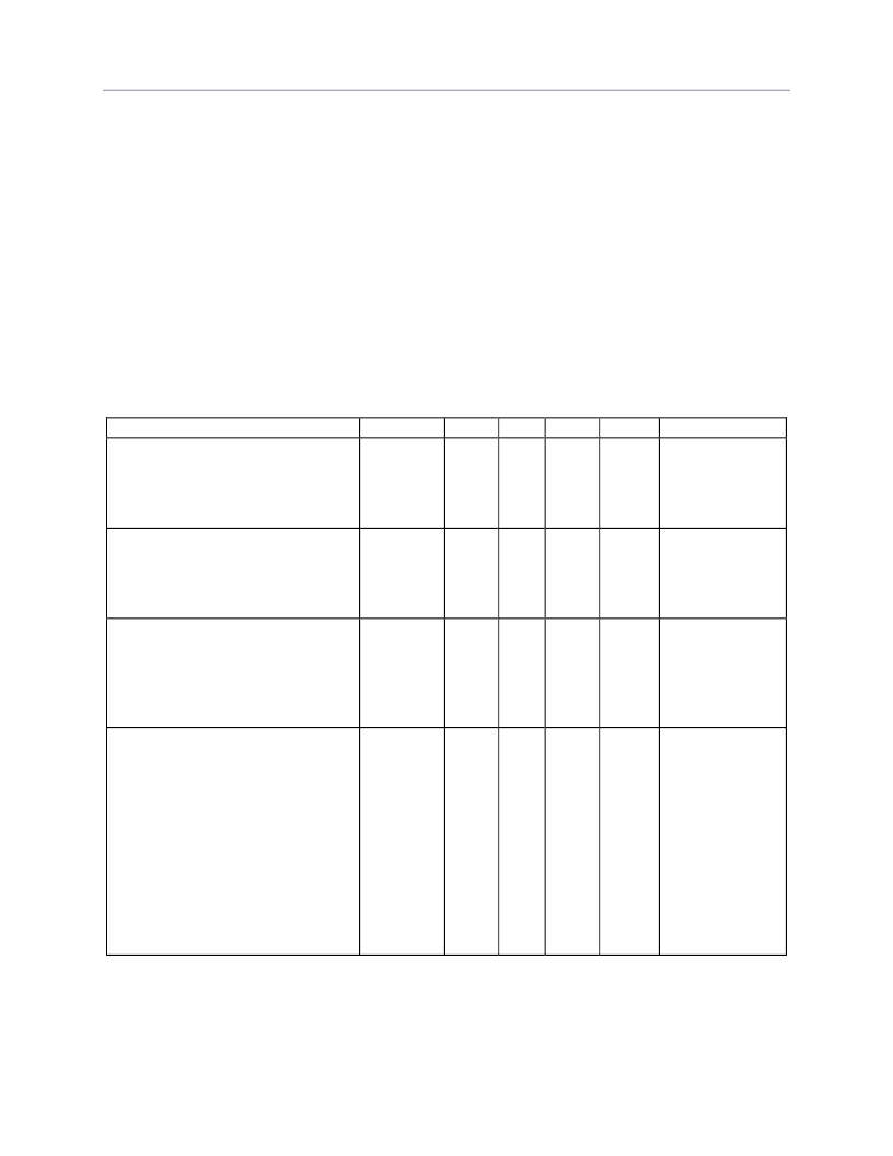
7.0 DC PARAMETERS
MAXIMUM GUARANTEED RATINGS
Operating Temperature Range...........................................................................................................................0
o
C to +70
o
C
Storage Temperature Range...........................................................................................................................-55
o
to +150
o
C
Lead Temperature Range (soldering, 10 seconds).....................................................................................................+325
o
C
Positive Voltage on any pin, with respect to Ground........................................................................................................5.5V
Negative Voltage on any pin, with respect to Ground .................................................................................................... -0.3V
Maximum
V
DDA,
V
DDIO
..................................................................................................................................................... +3.0V
Maximum
V
DD,
V
DDP
........................................................................................................................................................ +4.0V
*Stresses above the specified parameters could cause permanent damage to the device. This is a stress rating only
and functional operation of the device at any other condition above those indicated in the operation sections of this
specification is not implied.
Note:
When powering this device from laboratory or system power supplies, it is important that the Absolute Maximum
Ratings not be exceeded or device failure can result. Some power supplies exhibit voltage spikes on their outputs when
the AC power is switched on or off. In addition, voltage transients on the AC power line may appear on the DC output.
When this possibility exists, it is suggested that a clamp circuit be used.
DC ELECTRICAL CHARACTERISTICS (T
A
= 0°C - 70°C,
V
DDIO,
V
DDA
=
+3.3 V
± 10%,
V
DD,
V
DDP
=
+2.5 V
± 10%,)
PARAMETER
SYMBOL
I Type Input Buffer
MIN
TYP
MAX
UNITS
COMMENTS
Low Input Level
High Input Level
ICLK Input Buffer
V
ILI
V
IHI
2.0
0.8
V
V
TTL Levels
Low Input Level
High Input Level
Input Leakage
(All I and IS buffers)
V
ILCK
V
IHCK
2.2
0.4
V
V
Low Input Leakage
High Input Leakage
O8 Type Buffer
I
IL
I
IH
-10
-10
+10
+10
uA
mA
V
IN
= 0
V
IN
=
V
DDIO
Low Output Level
High Output Level
Output Leakage
V
OL
V
OH
I
OL
2.4
-10
0.4
+10
V
V
uA
I
OL
= 8 mA @
V
DDIO
= 3.3V
I
OH
= -4mA @
V
DDIO
= 3.3V
V
IN
= 0 to
V
DDIO
(Note 1)
相關(guān)PDF資料 |
PDF描述 |
|---|---|
| USB97CFDC | USB FLOPPY DISK CONTROLLER |
| USH-1000-KS | Lamps for Photolithography |
| USH1000FAL2 | Lamps for Photolithography |
| USH1002FGL | Lamps for Photolithography |
| USH1002FNIL2 | Lamps for Photolithography |
相關(guān)代理商/技術(shù)參數(shù) |
參數(shù)描述 |
|---|---|
| USB97C243-JN-04 | 制造商:Rochester Electronics LLC 功能描述:- Bulk |
| USB97CFDC | 制造商:SMSC 制造商全稱:SMSC 功能描述:USB FLOPPY DISK CONTROLLER |
| USB97CFDC2-01 | 制造商:SMSC 制造商全稱:SMSC 功能描述:USB Floppy Disk Controller |
| USB97CFDC2-MN-01 | 功能描述:USB 接口集成電路 USB Floppy Disk CNTRL RoHS:否 制造商:Cypress Semiconductor 產(chǎn)品:USB 2.0 數(shù)據(jù)速率: 接口類型:SPI 工作電源電壓:3.15 V to 3.45 V 工作電源電流: 最大工作溫度:+ 85 C 安裝風(fēng)格:SMD/SMT 封裝 / 箱體:WLCSP-20 |
| USB97CFDC2-MV-01 | 功能描述:USB 接口集成電路 USB Floppy Disk CNTRL RoHS:否 制造商:Cypress Semiconductor 產(chǎn)品:USB 2.0 數(shù)據(jù)速率: 接口類型:SPI 工作電源電壓:3.15 V to 3.45 V 工作電源電流: 最大工作溫度:+ 85 C 安裝風(fēng)格:SMD/SMT 封裝 / 箱體:WLCSP-20 |
發(fā)布緊急采購,3分鐘左右您將得到回復(fù)。