- 您現(xiàn)在的位置:買賣IC網(wǎng) > PDF目錄383986 > USB97C243 (SMSC Corporation) capacitor Selection for Internal Regulator Output Pins PDF資料下載
參數(shù)資料
| 型號(hào): | USB97C243 |
| 廠商: | SMSC Corporation |
| 英文描述: | capacitor Selection for Internal Regulator Output Pins |
| 中文描述: | 電容的選擇內(nèi)部穩(wěn)壓器輸出引腳 |
| 文件頁數(shù): | 19/59頁 |
| 文件大?。?/td> | 385K |
| 代理商: | USB97C243 |
第1頁第2頁第3頁第4頁第5頁第6頁第7頁第8頁第9頁第10頁第11頁第12頁第13頁第14頁第15頁第16頁第17頁第18頁當(dāng)前第19頁第20頁第21頁第22頁第23頁第24頁第25頁第26頁第27頁第28頁第29頁第30頁第31頁第32頁第33頁第34頁第35頁第36頁第37頁第38頁第39頁第40頁第41頁第42頁第43頁第44頁第45頁第46頁第47頁第48頁第49頁第50頁第51頁第52頁第53頁第54頁第55頁第56頁第57頁第58頁第59頁
SMSC DS – USB97C201
Page 19
Rev. 03/25/2002
PRELIMINARY
6.1.4
MCU REGISTER DESCRIPTIONS
6.1.4.1
MCU Runtime Registers
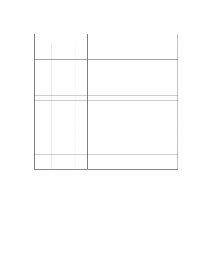
Table 6 - Interrupt 0 Source Register
ISR_0
(0x80 - RESET=0x0C)
BIT
7
USB_STAT
INTERRUPT 0 SOURCE REGISTER
DESCRIPTION
1= USB Bus System Event has occurred. Check USB_STAT
register for the specific event(s). This must be cleared by
clearing the USB_STAT register.
1= A SETUP packet was received on Endpoint 0. The EP0RX
bit of ISR_1 will not be set. If another SETUP packet is
received on Endpoint 0 while this bit is high, the bit will go low
and then immediately high again, to signal the duplicate
SETUP. If all other bits in this register are clear and the INT0
of the 8051is configured for edge triggering, then another
interrupt will be generated within the 8051. The firmware must
clear this bit by writing a "1" to it to allow the Enpoint 0 buffer
to receive subsequent data packets during the SETUP
transaction. Receipt of these packets will set EP0RX in ISR_1.
This bit always reads a “0”.
External interrupt input from the ATA-66 Interface.
1 = An ATA interrupt has occurred.
1 = The current transfer from the SRAM B Buffer has been
completed. See Sections 6.7 and 6.9 for more detail. This bit
is also cleared by writing a “1” to the RAMRD_TOGGLE bit of
the EP2_CTL register.
1 = The current transfer from the SRAM A Buffer has been
completed. See Sections 6.7 and 6.9 for more detail. . This bit
is also cleared by writing a “0” to the RAMRD_TOGGLE bit of
the EP2_CTL register.
1 = The current transfer to the SRAM B Buffer has been
completed. This bit may be cleared by the internal hardware
state machine while operating in “Auto Transfer” mode. See
Sections 6.7 and 6.9 for more detail.
1 = The current transfer to the SRAM A Buffer has been
completed. This bit may be cleared by the internal hardware
state machine while operating in “Auto Transfer” mode. See
Sections 6.7 and 6.9 for more detail.
NAME
R/W
R
6
SETUP
R/W
5
4
Reserved
ATA_IRQ
R
R/W
3
RAMRD_B
R/W
2
RAMRD_A
R/W
1
RAMWR_B
R/W
0
RAMWR_A
R/W
The bits in this register (except bit 7) are set to their POR values by writing a ‘1’ to the corresponding bit. If not
masked by the corresponding bit in the IMR0 mask register, a “1” on any of these bits will generate a “1” on the 8051
core’s external INT0 input.
相關(guān)PDF資料 |
PDF描述 |
|---|---|
| USB97CFDC | USB FLOPPY DISK CONTROLLER |
| USH-1000-KS | Lamps for Photolithography |
| USH1000FAL2 | Lamps for Photolithography |
| USH1002FGL | Lamps for Photolithography |
| USH1002FNIL2 | Lamps for Photolithography |
相關(guān)代理商/技術(shù)參數(shù) |
參數(shù)描述 |
|---|---|
| USB97C243-JN-04 | 制造商:Rochester Electronics LLC 功能描述:- Bulk |
| USB97CFDC | 制造商:SMSC 制造商全稱:SMSC 功能描述:USB FLOPPY DISK CONTROLLER |
| USB97CFDC2-01 | 制造商:SMSC 制造商全稱:SMSC 功能描述:USB Floppy Disk Controller |
| USB97CFDC2-MN-01 | 功能描述:USB 接口集成電路 USB Floppy Disk CNTRL RoHS:否 制造商:Cypress Semiconductor 產(chǎn)品:USB 2.0 數(shù)據(jù)速率: 接口類型:SPI 工作電源電壓:3.15 V to 3.45 V 工作電源電流: 最大工作溫度:+ 85 C 安裝風(fēng)格:SMD/SMT 封裝 / 箱體:WLCSP-20 |
| USB97CFDC2-MV-01 | 功能描述:USB 接口集成電路 USB Floppy Disk CNTRL RoHS:否 制造商:Cypress Semiconductor 產(chǎn)品:USB 2.0 數(shù)據(jù)速率: 接口類型:SPI 工作電源電壓:3.15 V to 3.45 V 工作電源電流: 最大工作溫度:+ 85 C 安裝風(fēng)格:SMD/SMT 封裝 / 箱體:WLCSP-20 |
發(fā)布緊急采購,3分鐘左右您將得到回復(fù)。