- 您現(xiàn)在的位置:買賣IC網(wǎng) > PDF目錄98293 > TS83102G0BMGS (ATMEL CORP) 1-CH 10-BIT PROPRIETARY METHOD ADC, PARALLEL ACCESS, CBGA152 PDF資料下載
參數(shù)資料
| 型號(hào): | TS83102G0BMGS |
| 廠商: | ATMEL CORP |
| 元件分類: | ADC |
| 英文描述: | 1-CH 10-BIT PROPRIETARY METHOD ADC, PARALLEL ACCESS, CBGA152 |
| 封裝: | HERMATIC, CI-CGA-152 |
| 文件頁(yè)數(shù): | 30/52頁(yè) |
| 文件大小: | 1548K |
| 代理商: | TS83102G0BMGS |
第1頁(yè)第2頁(yè)第3頁(yè)第4頁(yè)第5頁(yè)第6頁(yè)第7頁(yè)第8頁(yè)第9頁(yè)第10頁(yè)第11頁(yè)第12頁(yè)第13頁(yè)第14頁(yè)第15頁(yè)第16頁(yè)第17頁(yè)第18頁(yè)第19頁(yè)第20頁(yè)第21頁(yè)第22頁(yè)第23頁(yè)第24頁(yè)第25頁(yè)第26頁(yè)第27頁(yè)第28頁(yè)第29頁(yè)當(dāng)前第30頁(yè)第31頁(yè)第32頁(yè)第33頁(yè)第34頁(yè)第35頁(yè)第36頁(yè)第37頁(yè)第38頁(yè)第39頁(yè)第40頁(yè)第41頁(yè)第42頁(yè)第43頁(yè)第44頁(yè)第45頁(yè)第46頁(yè)第47頁(yè)第48頁(yè)第49頁(yè)第50頁(yè)第51頁(yè)第52頁(yè)
36
5360A–BDC–06/05
TS83102G0BMGS
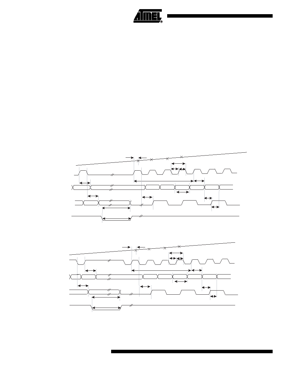
The DRRB’s rising edge occurs when the external encoding clock input (CLK/CLKB) is HIGH
: the Data Ready output’s first rising edge occurs after one clock period on the clock’s falling
edge, and a TDR delay time of 410 ps.
Consequently, as the analog input is sampled on the clock’s rising edge, the first digitized data
corresponding to the first acquisition (N), after a Data Ready signal restart (rising edge), is
always strobed by the third rising edge of the Data Ready signal.
The time delay (TD1) is specified between the last point of a change in the differential output
data (zero crossing point) to the rising or falling edge of the differential Data Ready signal
(DR/DRB) [zero crossing point].
Note:
For normal initialization of the Data Ready output signal, the external encoding clock signal fre-
quency and level must be controlled. The minimum encoding clock sampling rate for the ADC is
150 Msps, due to the internal Sample and Hold drop rate. Consequently the clock cannot be
stopped.
9.2.3
Timing Diagram
Figure 9-1.
TS83102G0BMGS Timing Diagram (2 Gsps Clock Rate) - Data Ready Reset Clock Held at LOW Level
Figure 9-2.
TS83102G0BMGS Timing Diagram (2 Gsps Clock Rate) - Data Ready Reset Clock Held at HIGH Level
N - 4
N - 3
N - 2
N - 1
N
N + 1
VIN/VINB
CLK/CLKB
Digital
Outputs
Data Ready
DR/DRB
Data Ready
Reset
TA = 160 ps
N
N + 1
N + 2
N + 3
N - 5
TOD = 360 ps
TDR = 410 ps
TRDR = 1000 ps
1 ns
TC = 500 ps
TC1 TC2
TPD = 4.0 Clock Period
TOD = 360 ps
500 ps
TDR = 410 ps
TD1 = TC1 + TDR - TOD
= TC1 + 50 ps = 300 ps
TD2 = TC2 + TOD - TDR
= TC2 - 50 ps = 200 ps
N - 4
N - 3
N - 2
N - 1
N
N + 1
N - 5
500 ps
TD2 = TC2 + TOD - TDR
= TC2 - 50 ps = 200 ps
TD1 = TC1 + TDR - TOD
= TC1 + 50 ps = 300 ps
TDR = 410 ps
TPD = 4.0 Clock Periods
TOD = 360 ps
TRDR = 1000 ps
1 ns
TDR = 410 ps
TOD = 360 ps
TA = 160 ps
N
N + 1
N + 2
N + 3
TC = 500 ps
TC1
TC2
VIN/VINB
CLK/CLKB
Digital
Outputs
Data Ready
DR/DRB
Data Ready
Reset
相關(guān)PDF資料 |
PDF描述 |
|---|---|
| TS83102G0BVGL | 1-CH 10-BIT PROPRIETARY METHOD ADC, PARALLEL ACCESS, CBGA152 |
| TS83102G0BCGL | 1-CH 10-BIT PROPRIETARY METHOD ADC, PARALLEL ACCESS, CBGA152 |
| TS83110CZT | 1-CH 10-BIT PROPRIETARY METHOD ADC, PARALLEL ACCESS, CDFP28 |
| TS83110MZT | 1-CH 10-BIT PROPRIETARY METHOD ADC, PARALLEL ACCESS, CDFP28 |
| TS83110VZT | 1-CH 10-BIT PROPRIETARY METHOD ADC, PARALLEL ACCESS, CDFP28 |
相關(guān)代理商/技術(shù)參數(shù) |
參數(shù)描述 |
|---|---|
| TS83102G0BVGL | 制造商:e2v technologies 功能描述:ADC SGL 2GSPS 10-BIT PARALLEL 152CBGA - Trays |
| TS83102G0CGL | 制造商:未知廠家 制造商全稱:未知廠家 功能描述:Analog to Digital Converter |
| TS83102G0GSZR5 | 制造商:e2v technologies 功能描述:TS83102G0GSZR5 - Trays |
| TS831-3I | 制造商:STMICROELECTRONICS 制造商全稱:STMicroelectronics 功能描述:MICROPOWER VOLTAGE SUPERVISOR RESET ACTIVE LOW |
| TS831-3ID | 功能描述:監(jiān)控電路 2.71V Micropower AL RoHS:否 制造商:STMicroelectronics 監(jiān)測(cè)電壓數(shù): 監(jiān)測(cè)電壓: 欠電壓閾值: 過(guò)電壓閾值: 輸出類型:Active Low, Open Drain 人工復(fù)位:Resettable 監(jiān)視器:No Watchdog 電池備用開(kāi)關(guān):No Backup 上電復(fù)位延遲(典型值):10 s 電源電壓-最大:5.5 V 最大工作溫度:+ 85 C 安裝風(fēng)格:SMD/SMT 封裝 / 箱體:UDFN-6 封裝:Reel |
發(fā)布緊急采購(gòu),3分鐘左右您將得到回復(fù)。