- 您現(xiàn)在的位置:買(mǎi)賣(mài)IC網(wǎng) > PDF目錄382649 > TMX320TCI6482ZTZA8 (Texas Instruments, Inc.) Communications Infrastructure Digital Signal Processor PDF資料下載
參數(shù)資料
| 型號(hào): | TMX320TCI6482ZTZA8 |
| 廠商: | Texas Instruments, Inc. |
| 元件分類(lèi): | 數(shù)字信號(hào)處理 |
| 英文描述: | Communications Infrastructure Digital Signal Processor |
| 中文描述: | 通信基礎(chǔ)設(shè)施的數(shù)字信號(hào)處理器 |
| 文件頁(yè)數(shù): | 4/255頁(yè) |
| 文件大小: | 1893K |
| 代理商: | TMX320TCI6482ZTZA8 |
第1頁(yè)第2頁(yè)第3頁(yè)當(dāng)前第4頁(yè)第5頁(yè)第6頁(yè)第7頁(yè)第8頁(yè)第9頁(yè)第10頁(yè)第11頁(yè)第12頁(yè)第13頁(yè)第14頁(yè)第15頁(yè)第16頁(yè)第17頁(yè)第18頁(yè)第19頁(yè)第20頁(yè)第21頁(yè)第22頁(yè)第23頁(yè)第24頁(yè)第25頁(yè)第26頁(yè)第27頁(yè)第28頁(yè)第29頁(yè)第30頁(yè)第31頁(yè)第32頁(yè)第33頁(yè)第34頁(yè)第35頁(yè)第36頁(yè)第37頁(yè)第38頁(yè)第39頁(yè)第40頁(yè)第41頁(yè)第42頁(yè)第43頁(yè)第44頁(yè)第45頁(yè)第46頁(yè)第47頁(yè)第48頁(yè)第49頁(yè)第50頁(yè)第51頁(yè)第52頁(yè)第53頁(yè)第54頁(yè)第55頁(yè)第56頁(yè)第57頁(yè)第58頁(yè)第59頁(yè)第60頁(yè)第61頁(yè)第62頁(yè)第63頁(yè)第64頁(yè)第65頁(yè)第66頁(yè)第67頁(yè)第68頁(yè)第69頁(yè)第70頁(yè)第71頁(yè)第72頁(yè)第73頁(yè)第74頁(yè)第75頁(yè)第76頁(yè)第77頁(yè)第78頁(yè)第79頁(yè)第80頁(yè)第81頁(yè)第82頁(yè)第83頁(yè)第84頁(yè)第85頁(yè)第86頁(yè)第87頁(yè)第88頁(yè)第89頁(yè)第90頁(yè)第91頁(yè)第92頁(yè)第93頁(yè)第94頁(yè)第95頁(yè)第96頁(yè)第97頁(yè)第98頁(yè)第99頁(yè)第100頁(yè)第101頁(yè)第102頁(yè)第103頁(yè)第104頁(yè)第105頁(yè)第106頁(yè)第107頁(yè)第108頁(yè)第109頁(yè)第110頁(yè)第111頁(yè)第112頁(yè)第113頁(yè)第114頁(yè)第115頁(yè)第116頁(yè)第117頁(yè)第118頁(yè)第119頁(yè)第120頁(yè)第121頁(yè)第122頁(yè)第123頁(yè)第124頁(yè)第125頁(yè)第126頁(yè)第127頁(yè)第128頁(yè)第129頁(yè)第130頁(yè)第131頁(yè)第132頁(yè)第133頁(yè)第134頁(yè)第135頁(yè)第136頁(yè)第137頁(yè)第138頁(yè)第139頁(yè)第140頁(yè)第141頁(yè)第142頁(yè)第143頁(yè)第144頁(yè)第145頁(yè)第146頁(yè)第147頁(yè)第148頁(yè)第149頁(yè)第150頁(yè)第151頁(yè)第152頁(yè)第153頁(yè)第154頁(yè)第155頁(yè)第156頁(yè)第157頁(yè)第158頁(yè)第159頁(yè)第160頁(yè)第161頁(yè)第162頁(yè)第163頁(yè)第164頁(yè)第165頁(yè)第166頁(yè)第167頁(yè)第168頁(yè)第169頁(yè)第170頁(yè)第171頁(yè)第172頁(yè)第173頁(yè)第174頁(yè)第175頁(yè)第176頁(yè)第177頁(yè)第178頁(yè)第179頁(yè)第180頁(yè)第181頁(yè)第182頁(yè)第183頁(yè)第184頁(yè)第185頁(yè)第186頁(yè)第187頁(yè)第188頁(yè)第189頁(yè)第190頁(yè)第191頁(yè)第192頁(yè)第193頁(yè)第194頁(yè)第195頁(yè)第196頁(yè)第197頁(yè)第198頁(yè)第199頁(yè)第200頁(yè)第201頁(yè)第202頁(yè)第203頁(yè)第204頁(yè)第205頁(yè)第206頁(yè)第207頁(yè)第208頁(yè)第209頁(yè)第210頁(yè)第211頁(yè)第212頁(yè)第213頁(yè)第214頁(yè)第215頁(yè)第216頁(yè)第217頁(yè)第218頁(yè)第219頁(yè)第220頁(yè)第221頁(yè)第222頁(yè)第223頁(yè)第224頁(yè)第225頁(yè)第226頁(yè)第227頁(yè)第228頁(yè)第229頁(yè)第230頁(yè)第231頁(yè)第232頁(yè)第233頁(yè)第234頁(yè)第235頁(yè)第236頁(yè)第237頁(yè)第238頁(yè)第239頁(yè)第240頁(yè)第241頁(yè)第242頁(yè)第243頁(yè)第244頁(yè)第245頁(yè)第246頁(yè)第247頁(yè)第248頁(yè)第249頁(yè)第250頁(yè)第251頁(yè)第252頁(yè)第253頁(yè)第254頁(yè)第255頁(yè)
www.ti.com
1.3
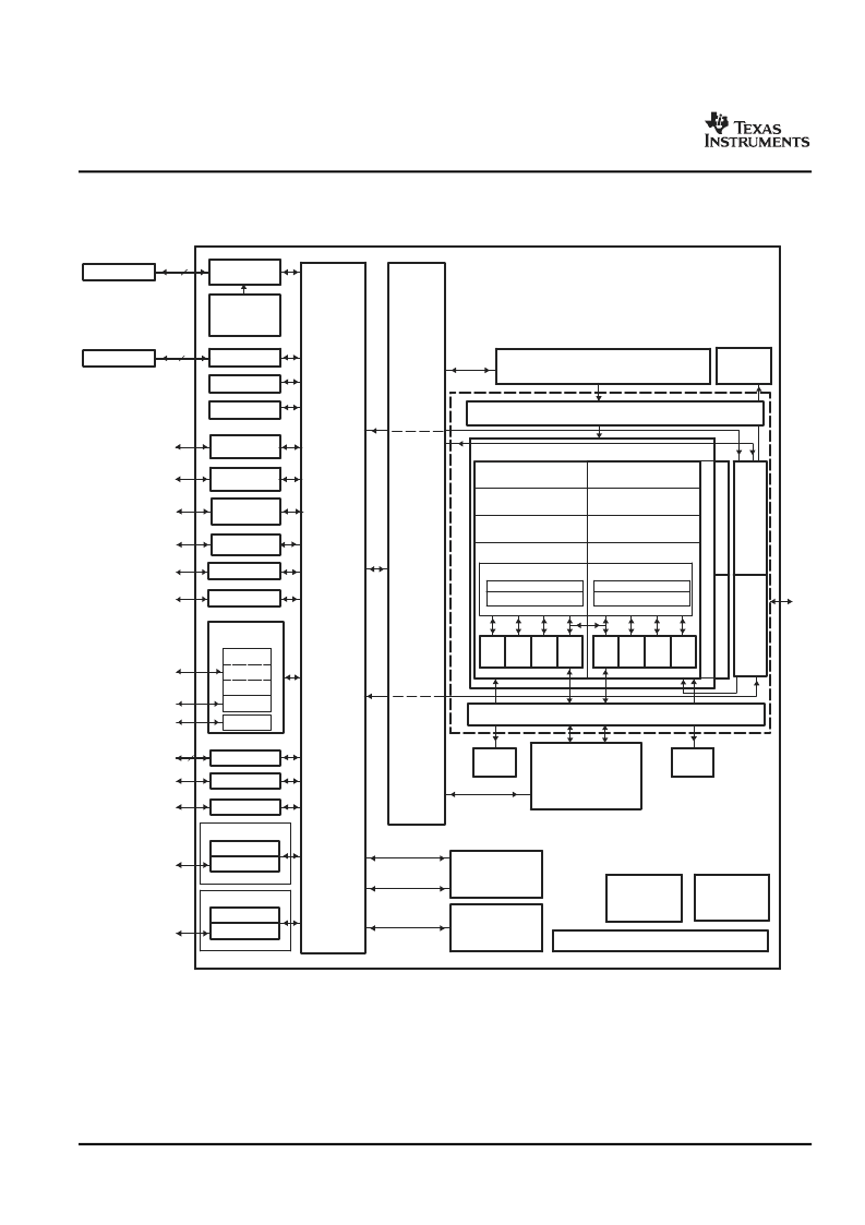
Functional Block Diagram
MDIO
EMAC
10/100/1000
Serial Rapid
I/O
DDR2
Mem Ctlr
Device
Configuration
Logic
64
L1P SRAM/Cache Direct-Mapped
32K Bytes
L1D SRAM/Cache
2-Way
Set-Associative
32K Bytes Total
TCI6482
PLL1 and
PLL1
Controller
EMIFA
HI
LO
Boot Configuration
I/O Devices
UTOPIA
(B)
VCP2
I2C
GPIO16
(B)
16
McBSP0
(A)
RSA
RSA
RMGII
(D)
L2
Cache
Memory
2096K
Bytes
L2 ROM
32K
Bytes
(E)
TCP2
McBSP1
(A)
HPI (32/16)
(B)
A. McBSPs: Framing Chips H.100, MVIP, SCSA, T1, E1; AC97 Devices; SPI Devices; Codecs
B. The PCI peripheral pins are muxed with some of the HPI peripheral pins and the UTOPIA address pins. For more detailed information, see the
Device
Configuration
section of this document.
C. Each of the TIMER peripherals (TIMER1 and TIMER0) is configurable as either two 64-bit general-purpose timers
or
two 32-bit general-purpose
timers
or
a watchdog timer.
D. The PLL2 controller also generates clocks for the EMAC.
E. When accessing the internal ROM of the DSP, the CPU frequency must always be less than 750 MHz.
DDR2 SDRAM
32
Timer1
(C)
HI
LO
Timer0
(C)
PCI66
(B)
VLYNQ
PLL2 and
PLL2
Controller
(D)
GMII
RMII
MII
P
EDMA 3.0
L
(
B
S
C64x+ DSP Core
Data Path B
B Register File
B31B16
B15B0
Instruction Fetch
Data Path A
A Register File
A31A16
A15A0
.L1
.S1
.M1
xx
xx
.D1
.D2
.M2
xx
xx
.S2
.L2
I
(
M
e
g
a
m
o
d
u
l
e
L1P Memory Controller (Memory Protect/Bandwidth Mgmt)
Instruction
Decode
16-/32-bit
Instruction Dispatch
Control Registers
In-Circuit Emulation
SPLOOP Buffer
P
L1D Memory Controller (Memory Protect/Bandwidth Mgmt)
I
Secondary
Switched Central
Resource
TMS320TCI6482
Communications Infrastructure Digital Signal Processor
SPRS246F–APRIL 2005–REVISED MAY 2007
Figure 1-2
shows the functional block diagram of the TCI6482 device.
Figure 1-2. Functional Block Diagram
Features
4
Submit Documentation Feedback
相關(guān)PDF資料 |
PDF描述 |
|---|---|
| TMX380SRAFNL | Communications Interface |
| TMX70A2400AJDL | Modem Controller |
| TMX99532NL | MODEM |
| TMXF281553BAL-3C-DB | Telecomm/Datacomm |
| TFRA28J133BAL-1 | Transient Voltage Suppressor Diodes |
相關(guān)代理商/技術(shù)參數(shù) |
參數(shù)描述 |
|---|---|
| TMX320TCI6616XCYP | 制造商:Texas Instruments 功能描述: |
| TMX320VC33PGE | 制造商:Texas Instruments 功能描述: |
| TMX320VC5401PGE50 | 制造商:Rochester Electronics LLC 功能描述:- Bulk |
| TMX320VC5402GGLL100 | 制造商:Rochester Electronics LLC 功能描述:- Bulk |
| TMX320VC5402GGU100 | 制造商:Rochester Electronics LLC 功能描述:- Bulk |
發(fā)布緊急采購(gòu),3分鐘左右您將得到回復(fù)。