- 您現(xiàn)在的位置:買賣IC網(wǎng) > PDF目錄371187 > TMPR28051 TMPR28051 STS-1/AU-3 (STM-0) Mapper Device Advisory for Version 5 of the Device PDF資料下載
參數(shù)資料
| 型號: | TMPR28051 |
| 英文描述: | TMPR28051 STS-1/AU-3 (STM-0) Mapper Device Advisory for Version 5 of the Device |
| 中文描述: | TMPR28051 STS-1/AU-3(的STM - 0)映射為版本的設(shè)備5設(shè)備咨詢 |
| 文件頁數(shù): | 63/90頁 |
| 文件大小: | 1090K |
| 代理商: | TMPR28051 |
第1頁第2頁第3頁第4頁第5頁第6頁第7頁第8頁第9頁第10頁第11頁第12頁第13頁第14頁第15頁第16頁第17頁第18頁第19頁第20頁第21頁第22頁第23頁第24頁第25頁第26頁第27頁第28頁第29頁第30頁第31頁第32頁第33頁第34頁第35頁第36頁第37頁第38頁第39頁第40頁第41頁第42頁第43頁第44頁第45頁第46頁第47頁第48頁第49頁第50頁第51頁第52頁第53頁第54頁第55頁第56頁第57頁第58頁第59頁第60頁第61頁第62頁當(dāng)前第63頁第64頁第65頁第66頁第67頁第68頁第69頁第70頁第71頁第72頁第73頁第74頁第75頁第76頁第77頁第78頁第79頁第80頁第81頁第82頁第83頁第84頁第85頁第86頁第87頁第88頁第89頁第90頁
Data Sheet
August 1999
TMPR28051 STS-1/AU-3 (STM-0) Mapper
49
Lucent Technologies Inc.
Microprocessor Interface Description
(continued)
Register Architecture Description
(continued)
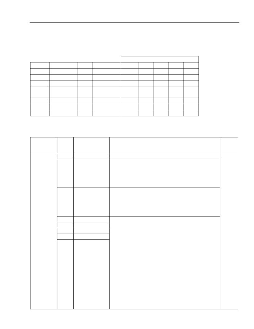
Table 17. DS1/E1 Insertion Selection Format
VT Drop Selection (0x33—0x4E)
Table 18. Registers 0x33—0x4E: VT Drop Selection
5 Programmed DS1/E1INS[4:0]_x Bits
Bit 4
Bit 3
Bit 2
0
0
0
0
0
0
1
1
1
1
1
1
VT1.5 #
1
2
3
26
27
28
VT Group #
1
2
3
5
6
7
VT #
1
1
1
4
4
4
Address
17
18
19
30
31
32
Bit 1
0
1
1
1
1
0
Bit 0
1
0
1
0
1
0
0
0
0
0
0
1
Address
(Hex)
Bit #
Name
Function
Reset
Default
(Hex)
Value is
0.
0x33—0x4E
7
6
—
Reserved.
The RXESOF[1:28] bits (see VT Drop Selection Registers,
Table 14, page 25) report the receive elastic store overflow
condition. When any of these bits is 1, the corresponding
DS1/E1 output has experienced an elastic store overflow.
This value is latched by these bits until read by the micro-
processor.
The TXESOF[1:28] bits (see Control, Alarm, and Mask Bit
Registers, Table 14, page 23) report the transmit elastic
store overflow condition. When any of these bits is 1, the
corresponding DS1/E1 input has experienced an elastic
store overflow. This value is latched by these bits until read
by the microprocessor.
VTDROP4_[1:28] These bits in registers 0x33—0x4E are used to select the
VT1.5 slot for the DS1/E1 outputs. The VT1.5 selected in
Table 17 corresponds to the decimal value of these pro-
grammed 5 bits. If these bits contain 00000, or 11101—
11111, then the device inserts the following:
VTDROP0_[1:28]
RXESOF[1:28]
5
TXESOF[1:28]
4
3
2
1
0
00000 = device does not transmit any clock or data
11101 = device inserts a DS1 AIS into the corresponding
DS1/E1 slot
11110 = device inserts a E1 AIS into the corresponding
DS1/E1 slot
11111= device inserts the test pattern
Since the device defaults these bits in all 28 of these regis-
ters to 00000, there will be no clock or data in any of the
28 DS1 or 21 E1 slots after reset. VTDROP[4:0]_[1:28],
bits 00001—11100, correspond to the specific VT1.5
streams as shown in Table , page 50. Address 0x33—
0x4E correspond to VTs as shown in Table 20, also on
page 50.
VTDROP3_[1:28]
VTDROP2_[1:28]
VTDROP1_[1:28]
相關(guān)PDF資料 |
PDF描述 |
|---|---|
| TMUX03155 | TMUX03155 STS-3/STM-1 (AU-4) Multiplexer/Demultiplexer |
| TMXF28155 | TMXF28155 Super Mapper 155/51 Mbits/s SONET/SDH x28/x21 DS1/E1 |
| TMXF84622 | TMXF84622 155 Mbits/s/622 Mbits/s Interface SONET/SDH x84/x63 Ultramapper |
| TN2-L-H-3V | SLIM POLARIZED RELAY |
| TN2-L-H-48V | SLIM POLARIZED RELAY |
相關(guān)代理商/技術(shù)參數(shù) |
參數(shù)描述 |
|---|---|
| TMPR28051-3-SL5 | 制造商:AGERE 制造商全稱:AGERE 功能描述:TMPR28051 STS-1/AU-3 (STM-0) Mapper Device Advisory for Version 5 of the Device |
| TMPR28051-SL | 制造商:未知廠家 制造商全稱:未知廠家 功能描述:ATM/SONET MAPPER|QFP|208PIN|PLASTIC |
| TMPR3904F | 制造商:未知廠家 制造商全稱:未知廠家 功能描述:MICROPROCESSOR|32-BIT|CMOS|QFP|208PIN|PLASTIC |
| TMPR3907F | 制造商:未知廠家 制造商全稱:未知廠家 功能描述:MICROPROCESSOR|32-BIT|CMOS|QFP|208PIN|PLASTIC |
| TMPR3911 | 制造商:TOSHIBA 制造商全稱:Toshiba Semiconductor 功能描述:32-Bit TX System RISC TX39 Family |
發(fā)布緊急采購,3分鐘左右您將得到回復(fù)。