- 您現(xiàn)在的位置:買賣IC網(wǎng) > PDF目錄383959 > TM248GBK32-80 (Texas Instruments, Inc.) DYNAMIC RAM MODULES PDF資料下載
參數(shù)資料
| 型號(hào): | TM248GBK32-80 |
| 廠商: | Texas Instruments, Inc. |
| 英文描述: | DYNAMIC RAM MODULES |
| 中文描述: | 動(dòng)態(tài)隨機(jī)存儲(chǔ)器模塊 |
| 文件頁數(shù): | 7/11頁 |
| 文件大小: | 158K |
| 代理商: | TM248GBK32-80 |
TM124FBK32, TM124FBK32S 1048576 BY 32-BIT
TM248GBK32, TM248GBK32S 2097152 BY 32-BIT
DYNAMIC RAMMODULES
SMMS664A – DECEMBER 1995 – REVISED JUNE 1996
7
POST OFFICE BOX 1443
HOUSTON, TEXAS 77251–1443
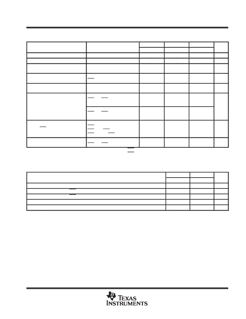
electrical characteristics over full ranges of recommended operating conditions (unless otherwise
noted)
PARAMETER
TEST CONDITIONS
’248GBK32-60
MIN
2.4
’248GBK32-70
MIN
2.4
’248GBK32-80
MIN
2.4
UNIT
MAX
MAX
MAX
VOH
VOL
High-level output voltage
IOH = – 5 mA
IOL = 4.2 mA
VI = 0 to 6.5 V,
All other pins = 0 to VCC
VO = 0 to VCC,
CAS high
V
Low-level output voltage
0.4
0.4
0.4
V
II
Input current (leakage)
VCC = 5 V,
±
20
±
20
±
20
μ
A
IO
Output current (leakage)
VCC = 5.5 V,
±
20
±
20
±
20
μ
A
ICC1
Read- or write-cycle current
(see Note 3)
Minimum cycle,
VCC = 5.5 V
856
736
656
mA
ICC1
Standby current
After one memory cycle,
RAS and CAS high,
VIH=2.4 V (TTL)
After one memory cycle,
RAS and CAS high,
VIH = VCC – 0.2 V (CMOS)
Minimum cycle,
RAS cycling,
CAS high (RAS-only),
RAS low after CAS low (CBR)
32
32
32
mA
16
16
16
ICC3
Average refresh current
(RAS-only or CBR)
(see Note 3)
VCC = 5.5 V,
1680
1440
1280
mA
ICC4
Average EDO current
(see Note 4)
tPC = minimum,
RAS low, CAS cycling
VCC = 5.5 V,
736
656
576
mA
NOTES:
3. Measured with a maximum of one address change while RAS = VIL.
4. Measured with a maximum of one address change while CAS = VIH.
capacitance over recommended ranges of supply voltage and operating free-air temperature
f = 1 MHz (see Note 5)
’124FBK32
MIN
’248GBK32
MIN
UNIT
MAX
MAX
Ci(A)
Ci(R)
Ci(C)
Ci(W)
Co(DQ)
NOTE 5: VCC equal to 5 V
±
0.5 V and the bias on pins under test is 0 V.
Input capacitance, address inputs
40
80
pF
Input capacitance, RAS
28
28
pF
Input capacitance, CAS
14
28
pF
Input capacitance, write-enable input
56
112
pF
Output capacitance on DQ pins
7
14
pF
相關(guān)PDF資料 |
PDF描述 |
|---|---|
| TMC2072KHC | Genlocking Video Digitizer |
| TMC2072 | Genlocking Video Digitizer |
| TMC2192KHC | 10 Bit Encoder |
| TMC2193KJC | 10 Bit Encoder |
| TMC2193 | 10 Bit Encoder |
相關(guān)代理商/技術(shù)參數(shù) |
參數(shù)描述 |
|---|---|
| TM248GBK32S-60 | 制造商:TI 制造商全稱:Texas Instruments 功能描述:DYNAMIC RAM MODULES |
| TM248GBK32S-70 | 制造商:TI 制造商全稱:Texas Instruments 功能描述:DYNAMIC RAM MODULES |
| TM248GBK32S-80 | 制造商:TI 制造商全稱:Texas Instruments 功能描述:DYNAMIC RAM MODULES |
| TM248NBK36B | 制造商:TI 制造商全稱:Texas Instruments 功能描述:DYNAMIC RAM MODULE |
| TM248NBK36B-60 | 制造商:TI 制造商全稱:Texas Instruments 功能描述:DYNAMIC RAM MODULE |
發(fā)布緊急采購,3分鐘左右您將得到回復(fù)。