- 您現(xiàn)在的位置:買賣IC網(wǎng) > PDF目錄98255 > TLV320DAC3100IRHBR (TEXAS INSTRUMENTS INC) DAC WITH PROGRAMMABLE PLL, PQCC32 PDF資料下載
參數(shù)資料
| 型號: | TLV320DAC3100IRHBR |
| 廠商: | TEXAS INSTRUMENTS INC |
| 元件分類: | DAC |
| 英文描述: | DAC WITH PROGRAMMABLE PLL, PQCC32 |
| 封裝: | 5 X 5 MM, GREEN, PLASTIC, QFN-32 |
| 文件頁數(shù): | 55/97頁 |
| 文件大?。?/td> | 1134K |
| 代理商: | TLV320DAC3100IRHBR |
第1頁第2頁第3頁第4頁第5頁第6頁第7頁第8頁第9頁第10頁第11頁第12頁第13頁第14頁第15頁第16頁第17頁第18頁第19頁第20頁第21頁第22頁第23頁第24頁第25頁第26頁第27頁第28頁第29頁第30頁第31頁第32頁第33頁第34頁第35頁第36頁第37頁第38頁第39頁第40頁第41頁第42頁第43頁第44頁第45頁第46頁第47頁第48頁第49頁第50頁第51頁第52頁第53頁第54頁當(dāng)前第55頁第56頁第57頁第58頁第59頁第60頁第61頁第62頁第63頁第64頁第65頁第66頁第67頁第68頁第69頁第70頁第71頁第72頁第73頁第74頁第75頁第76頁第77頁第78頁第79頁第80頁第81頁第82頁第83頁第84頁第85頁第86頁第87頁第88頁第89頁第90頁第91頁第92頁第93頁第94頁第95頁第96頁第97頁
DA(6)
DA(0)
RA(7)
RA(0)
D(7)
D(0)
Start
(M)
7-bitDevice Address
(M)
Write
(M)
Slave
Ack
(S)
8-bitRegister Address
(M)
Slave
Ack
(S)
8-bitRegisterData
(M)
Stop
(M)
Slave
Ack
(S)
SDA
SCL
(M)=>SDA ControlledbyMaster
(S)=>SDA ControlledbySlave
www.ti.com
SLAS671 – FEBRUARY 2010
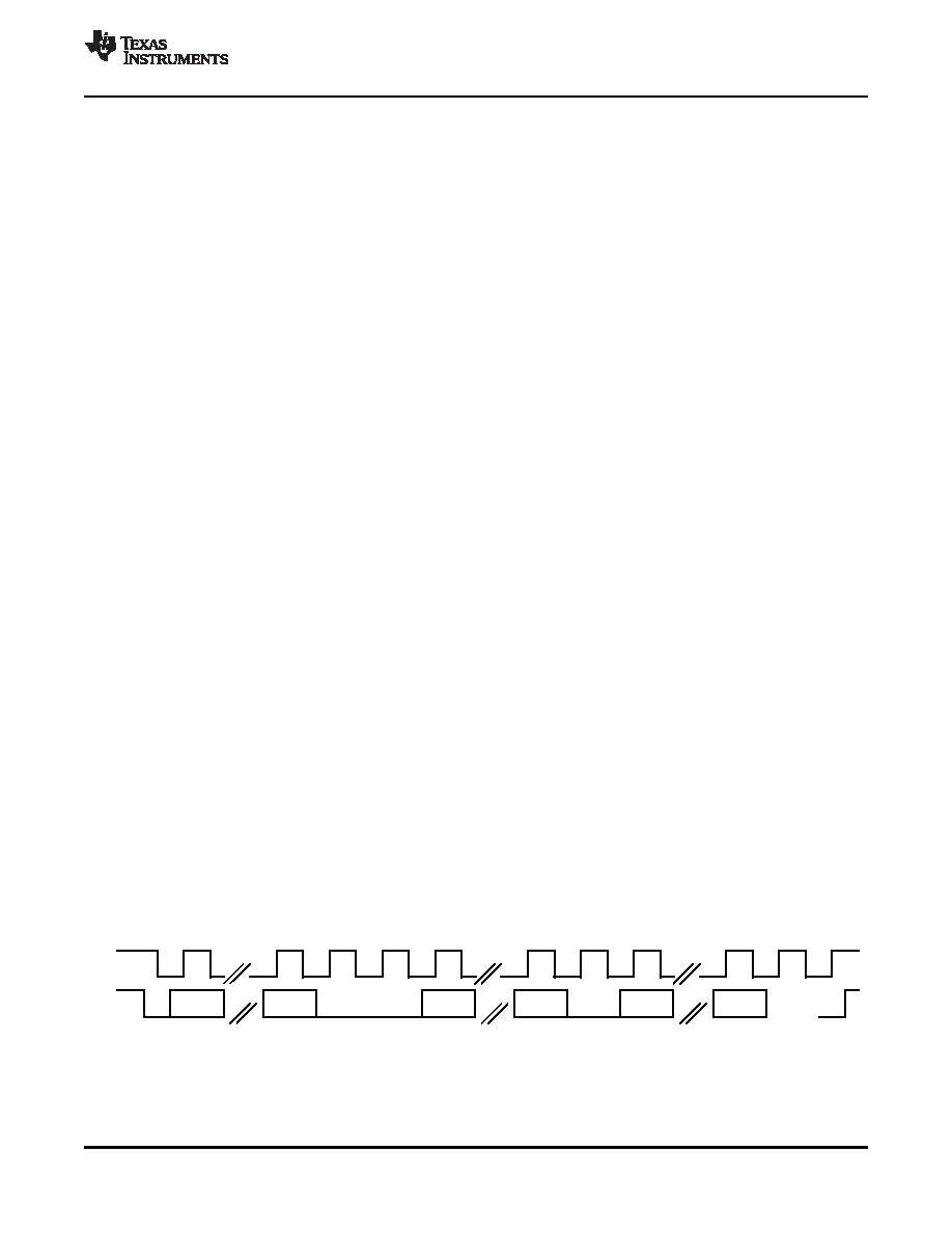
Communication on the I2C bus always takes place between two devices, one acting as the master and the
other acting as the slave. Both masters and slaves can read and write, but slaves can only do so under
the direction of the master. Some I2C devices can act as masters or slaves, but the TLV320DAC3100 can
only act as a slave device.
An I2C bus consists of two lines, SDA and SCL. SDA carries data, and the SCL signal provides the clock.
All data is transmitted across the I2C bus in groups of eight bits. To send a bit on the I2C bus, the SDA line
is driven to the appropriate level while SCL is LOW (a LOW on SDA indicates the bit is 0, whereas a
HIGH indicates the bit is 1).
Once the SDA line has settled, the SCL line is brought HIGH, then LOW. This pulse on the SCL line
clocks the SDA bit into the receiver shift register.
The I2C bus is bidirectional: the SDA line is used both for transmitting and receiving data. When a master
reads from a slave, the slave drives the data line; when a master sends to a slave, the master drives the
data line.
Most of the time the bus is idle, no communication is taking place, and both lines are HIGH. When
communication is taking place, the bus is active. Only master devices can start communication on the bus.
Normally, the data line is only allowed to change state while the clock line is LOW. If the data line changes
state while the clock line is HIGH, it is either a START condition or its counterpart, a STOP condition. A
START condition is when the clock line is HIGH and the data line goes from HIGH to LOW. A STOP
condition is when the clock line is HIGH and the data line goes from LOW to HIGH.
After the master issues a START condition, it sends a byte that selects the slave device for
communication. This byte is called the address byte. Each device on an I2C bus has a unique 7-bit
address to which it responds. (Slaves can also have 10-bit addresses; see the I2C specification for
details.) The master sends an address in the address byte, together with a bit that indicates whether it is
to read from or write to the slave device.
Every byte transmitted on the I2C bus, whether it is address or data, is acknowledged with an
acknowledge bit. When a master has finished sending a byte (eight data bits) to a slave, it stops driving
SDA and waits for the slave to acknowledge the byte. The slave acknowledges the byte by pulling SDA
LOW. The master then sends a clock pulse to clock the acknowledge bit. Similarly, when a master has
finished reading a byte, it pulls SDA LOW to acknowledge this to the slave. It then sends a clock pulse to
clock the bit. (Remember that the master always drives the clock line.)
A not-acknowledge is performed simply by leaving SDA HIGH during an acknowledge cycle. If a device is
not present on the bus and the master attempts to address it, it receives a not-acknowledge because no
device is present at that address to pull the line LOW.
When a master has finished communicating with a slave, it may issue a STOP condition. When a STOP
condition is issued, the bus becomes idle again. A master may also issue another START condition. When
a START condition is issued while the bus is active, it is called a repeated START condition.
The TLV320DAC3100 can also respond to and acknowledge a general call, which consists of the master
issuing a command with a slave address byte of 00h. This feature is disabled by default, but can be
enabled via page 0 / register 34, bit D5.
Figure 5-34. I2C Write
Copyright 2010, Texas Instruments Incorporated
APPLICATION INFORMATION
59
Product Folder Link(s): TLV320DAC3100
相關(guān)PDF資料 |
PDF描述 |
|---|---|
| TLV320DAC3100IRHBT | DAC WITH PROGRAMMABLE PLL, PQCC32 |
| TLV320DAC3101IRHBT | DAC WITH PROGRAMMABLE PLL, PQCC32 |
| TLV320DAC3101IRHBR | DAC WITH PROGRAMMABLE PLL, PQCC32 |
| TLV320DAC3120IRHBR | SERIAL INPUT LOADING, 24-BIT DAC, PQCC32 |
| TLV320DAC3120IRHBT | SERIAL INPUT LOADING, 24-BIT DAC, PQCC32 |
相關(guān)代理商/技術(shù)參數(shù) |
參數(shù)描述 |
|---|---|
| TLV320DAC3100IRHBT | 功能描述:音頻數(shù)/模轉(zhuǎn)換器 IC Low-Pwr Stereo Audio DAC RoHS:否 制造商:Texas Instruments 轉(zhuǎn)換器數(shù)量: 分辨率:16 bit 接口類型:I2S, UBS 轉(zhuǎn)換速率: 信噪比:98 dB 工作電源電壓:5 V DAC 輸出端數(shù)量:2 工作溫度范圍:- 25 C to + 85 C 電源電流:23 mA 安裝風(fēng)格:SMD/SMT 封裝 / 箱體:TQFP-32 封裝:Reel |
| TLV320DAC3101 | 制造商:TI 制造商全稱:Texas Instruments 功能描述:Low-Power Stereo Audio DAC With Audio Processing and Stereo Class-D Speaker Amplifier |
| TLV320DAC3101EVM-U | 功能描述:音頻 IC 開發(fā)工具 TLV320DAC3101EVM-U Eval Mod RoHS:否 制造商:Texas Instruments 產(chǎn)品:Evaluation Kits 類型:Audio Amplifiers 工具用于評估:TAS5614L 工作電源電壓:12 V to 38 V |
| TLV320DAC3101IRHBR | 功能描述:音頻數(shù)/模轉(zhuǎn)換器 IC Low-Pwr audio DAC RoHS:否 制造商:Texas Instruments 轉(zhuǎn)換器數(shù)量: 分辨率:16 bit 接口類型:I2S, UBS 轉(zhuǎn)換速率: 信噪比:98 dB 工作電源電壓:5 V DAC 輸出端數(shù)量:2 工作溫度范圍:- 25 C to + 85 C 電源電流:23 mA 安裝風(fēng)格:SMD/SMT 封裝 / 箱體:TQFP-32 封裝:Reel |
| TLV320DAC3101IRHBT | 功能描述:音頻數(shù)/模轉(zhuǎn)換器 IC Low-Pwr audio DAC RoHS:否 制造商:Texas Instruments 轉(zhuǎn)換器數(shù)量: 分辨率:16 bit 接口類型:I2S, UBS 轉(zhuǎn)換速率: 信噪比:98 dB 工作電源電壓:5 V DAC 輸出端數(shù)量:2 工作溫度范圍:- 25 C to + 85 C 電源電流:23 mA 安裝風(fēng)格:SMD/SMT 封裝 / 箱體:TQFP-32 封裝:Reel |
發(fā)布緊急采購,3分鐘左右您將得到回復(fù)。