- 您現(xiàn)在的位置:買賣IC網(wǎng) > PDF目錄384008 > TLV2211Y (Texas Instruments, Inc.) Advanced LinCMOSE RAIL-TO-RAIL MICROPOWER SINGLE OPERATIONAL AMPLIFIERS PDF資料下載
參數(shù)資料
| 型號(hào): | TLV2211Y |
| 廠商: | Texas Instruments, Inc. |
| 英文描述: | Advanced LinCMOSE RAIL-TO-RAIL MICROPOWER SINGLE OPERATIONAL AMPLIFIERS |
| 中文描述: | 高級(jí)LinCMOSE軌至軌微功耗單運(yùn)算放大器 |
| 文件頁(yè)數(shù): | 1/29頁(yè) |
| 文件大?。?/td> | 529K |
| 代理商: | TLV2211Y |
當(dāng)前第1頁(yè)第2頁(yè)第3頁(yè)第4頁(yè)第5頁(yè)第6頁(yè)第7頁(yè)第8頁(yè)第9頁(yè)第10頁(yè)第11頁(yè)第12頁(yè)第13頁(yè)第14頁(yè)第15頁(yè)第16頁(yè)第17頁(yè)第18頁(yè)第19頁(yè)第20頁(yè)第21頁(yè)第22頁(yè)第23頁(yè)第24頁(yè)第25頁(yè)第26頁(yè)第27頁(yè)第28頁(yè)第29頁(yè)
TLV2211, TLV2211Y
Advanced LinCMOS
RAIL-TO-RAIL
MICROPOWER SINGLE OPERATIONAL AMPLIFIERS
SLOS156B – MAY 1996 – REVISED JANUARY 1997
1
POST OFFICE BOX 655303
DALLAS, TEXAS 75265
Output Swing Includes Both Supply Rails
Low Noise . . . 21 nV/
√
Hz Typ at f = 1 kHz
Low Input Bias Current . . . 1 pA Typ
Very Low Power . . . 13
μ
A Per Channel Typ
Common-Mode Input Voltage Range
Includes Negative Rail
Wide Supply Voltage Range
2.7 V to 10 V
Available in the SOT-23 Package
Macromodel Included
description
The TLV2211 is a single operational amplifier manufactured using the Texas Instruments Advanced LinCMOS
process. These devices are optimized and fully specified for single-supply 3-V and 5-V operation. For this
low-voltage operation combined with micropower dissipation levels, the input noise voltage performance has
been dramatically improved using optimized design techniques for CMOS-type amplifiers. Another added
benefit is that these amplifiers exhibit rail-to-rail output swing. The output dynamic range can be extended using
the TLV2211 with loads referenced midway between the rails. The common-mode input voltage range is wider
than typical standard CMOS-type amplifiers. To take advantage of this improvement in performance and to
make this device available for a wider range of applications, V
ICR
is specified with a larger maximum input offset
voltage test limit of
±
5 mV, allowing a minimum of 0 to 2-V common-mode input voltage range for a 3-V power
supply.
AVAILABLE OPTIONS
TA
VIOmax AT 25
°
C
PACKAGED DEVICES
SOT-23 (DBV)
TLV2211CDBV
TLV2211IDBV
SYMBOL
CHIP FORM
(Y)
0
°
C to 70
°
C
–40
°
C to 85
°
C
The DBV package available in tape and reel only.
3 mV
3 mV
VACC
VACI
TLV2211Y
The Advanced LinCMOS process uses a silicon-gate technology to obtain input offset voltage stability with
temperature and time that far exceeds that obtainable using metal-gate technology. This technology also makes
possible input-impedance levels that meet or exceed levels offered by top-gate JFET and expensive
dielectric-isolated devices.
The TLV2211, exhibiting high input impedance and low noise, is excellent for small-signal conditioning for
high-impedance sources such as piezoelectric transducers. Because of the low power dissipation levels
combined with 3-V operation, these devices work well in hand-held monitoring and remote-sensing
applications. In addition, the rail-to-rail output feature with single or split supplies makes these devices excellent
choices when interfacing directly to analog-to-digital converters (ADCs). All of these features combined with its
temperature performance make the TLV2211 ideal for remote pressure sensors, temperature control, active
voltage-resistive (VR) sensors, accelerometers, hand-held metering, and many other applications.
Please be aware that an important notice concerning availability, standard warranty, and use in critical applications of
Texas Instruments semiconductor products and disclaimers thereto appears at the end of this data sheet.
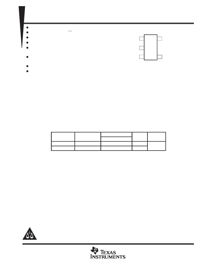
DBV PACKAGE
(TOP VIEW)
5
4
3
1
2
IN–
VDD–/GND
IN+
VDD+
OUT
PRODUCTION DATA information is current as of publication date.
Products conform to specifications per the terms of Texas Instruments
standard warranty. Production processing does not necessarily include
testing of all parameters.
Copyright
1997, Texas Instruments Incorporated
Advanced LinCMOS is a trademark of Texas Instruments Incorporated.
相關(guān)PDF資料 |
PDF描述 |
|---|---|
| TLV2221CDBV | Advanced LinCMOSE RAIL-TO-RAIL VERY LOW-POWER SINGLE OPERATIONAL AMPLIFIERS |
| TLV2221IDBV | Advanced LinCMOSE RAIL-TO-RAIL VERY LOW-POWER SINGLE OPERATIONAL AMPLIFIERS |
| TLV2221Y | Advanced LinCMOSE RAIL-TO-RAIL VERY LOW-POWER SINGLE OPERATIONAL AMPLIFIERS |
| TLV2231CDBV | Advanced LinCMOSE RAIL-TO-RAIL LOW-POWER SINGLE OPERATIONAL AMPLIFIERS |
| TLV2231IDBV | Advanced LinCMOSE RAIL-TO-RAIL LOW-POWER SINGLE OPERATIONAL AMPLIFIERS |
相關(guān)代理商/技術(shù)參數(shù) |
參數(shù)描述 |
|---|---|
| TLV2217 | 制造商:TI 制造商全稱:Texas Instruments 功能描述:LOW DROPOUT FIXED VOLTAGE REGULATORS |
| TLV2217_07 | 制造商:TI 制造商全稱:Texas Instruments 功能描述:LOW-DROPOUT FIXED-VOLTAGE REGULATOES |
| TLV2217-18 | 制造商:TI 制造商全稱:Texas Instruments 功能描述:LOW-DROPOUT FIXED-VOLTAGE REGULATOES |
| TLV2217-18KCS | 功能描述:低壓差穩(wěn)壓器 - LDO 1.8-V Fixed-Voltage RoHS:否 制造商:Texas Instruments 最大輸入電壓:36 V 輸出電壓:1.4 V to 20.5 V 回動(dòng)電壓(最大值):307 mV 輸出電流:1 A 負(fù)載調(diào)節(jié):0.3 % 輸出端數(shù)量: 輸出類型:Fixed 最大工作溫度:+ 125 C 安裝風(fēng)格:SMD/SMT 封裝 / 箱體:VQFN-20 |
| TLV2217-18KCSE3 | 功能描述:低壓差穩(wěn)壓器 - LDO 1.8-V Fixed-Voltage RoHS:否 制造商:Texas Instruments 最大輸入電壓:36 V 輸出電壓:1.4 V to 20.5 V 回動(dòng)電壓(最大值):307 mV 輸出電流:1 A 負(fù)載調(diào)節(jié):0.3 % 輸出端數(shù)量: 輸出類型:Fixed 最大工作溫度:+ 125 C 安裝風(fēng)格:SMD/SMT 封裝 / 箱體:VQFN-20 |
發(fā)布緊急采購(gòu),3分鐘左右您將得到回復(fù)。