- 您現(xiàn)在的位置:買賣IC網(wǎng) > PDF目錄384003 > TLC2543QEP (Texas Instruments, Inc.) 12-BIT ANALOG-TO-DIGITAL CONVERTER WITH SERIAL CONTROL AND 11 ANALOG INPUTS PDF資料下載
參數(shù)資料
| 型號: | TLC2543QEP |
| 廠商: | Texas Instruments, Inc. |
| 英文描述: | 12-BIT ANALOG-TO-DIGITAL CONVERTER WITH SERIAL CONTROL AND 11 ANALOG INPUTS |
| 中文描述: | 12位模擬數(shù)字轉(zhuǎn)換串行控制和11個模擬輸入 |
| 文件頁數(shù): | 4/25頁 |
| 文件大小: | 364K |
| 代理商: | TLC2543QEP |
www.ti.com
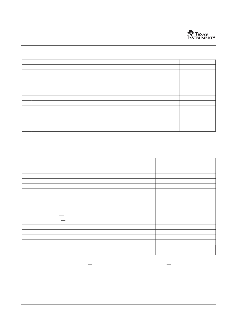
Absolute Maximum Ratings
(1)
over operating free-air temperature range (unless otherwise noted)
Recommended Operating Conditions
TLC2543-EP
12-BIT ANALOG-TO-DIGITAL CONVERTER
WITH SERIAL CONTROL AND 11 ANALOG INPUTS
SGLS125A–JULY 2002–REVISED NOVEMBER 2006
MIN
–0.5
MAX
6.5
V
CC
+
0.3
V
CC
+
0.3
V
CC
+
0.1
–0.1
±
20
±
30
125
125
150
260
UNIT
V
V
CC
Supply voltage range
(2)
V
I
Input voltage range (any input)
–0.3
V
V
O
Output voltage range
–0.3
V
V
ref+
Positive reference voltage
V
V
ref–
I
I
I
I
Negative reference voltage
Peak input current (any input)
Peak total input current (all inputs)
V
mA
mA
TLC2543Q
TLC2543M
–40
-55
–65
T
A
Operating free-air temperature range
°
C
T
stg
Storage temperature range
Lead temperature 1,6 mm (1/16 in) from the case for 10 s
°
C
°
C
(1)
Stresses beyond those listed under "absolute maximum ratings" may cause permanent damage to the device. These are stress ratings
only, and functional operation of the device at these or any other conditions beyond those indicated under "recommended operating
conditions" is not implied. Exposure to absolute-maximum-rated conditions for extended periods may affect device reliability.
All voltage values are with respect to the GND terminal with REF– and GND wired together (unless otherwise noted).
(2)
MIN
4.5
NOM
MAX
5.5
UNIT
V
V
V
V
V
V
V
MHz
ns
ns
ns
μ
s
ns
ns
μ
s
μ
s
V
CC
V
ref+
V
ref–
V
ref+
– V
ref–
Supply voltage
Positive reference voltage
(1)
Negative reference voltage
(1)
Differential reference voltage
(1)
Analog input voltage
(1)
High-level control input voltage
Low-level control input voltage
Clock frequency at I/O CLOCK
Setup time, address bits at DATA INPUT before I/O CLOCK
↑
(see
Figure 4
)
Hold time, address bits after I/O CLOCK
↑
(see
Figure 4
)
Hold time, CS low after last I/O CLOCK
↓
(see
Figure 5
)
Setup time, CS low before clocking in first address bit
(2)
(see
Figure 5
)
Pulse duration, I/O CLOCK high
Pulse duration, I/O CLOCK low
Transition time, I/O CLOCK high to low
(3)
(see
Figure 6
)
Transition time, DATA INPUT and CS
5
V
CC
0
2.5
V
CC
V
CC
+ 0.1
0
2
V
CC
V
IH
V
IL
V
CC
= 4.5 V to 5.5 V
V
CC
= 4.5 V to 5.5 V
0.8
4.1
0
t
su(A)
t
h(A)
t
h(CS)
t
su(CS)
t
wH(I/O)
t
wL(I/O)
t
t(I/O)
t
t(CS)
100
0
0
1.425
120
120
1
10
TLC2543Q
TLC2543M
–40
-55
125
125
T
A
Operating free-air temperature
°
C
(1)
Analog input voltages greater than that applied to REF+ convert as all ones (111111111111), while input voltages less than that applied
to REF– convert as all zeros (000000000000).
To minimize errors caused by noise at the CS input, the internal circuitry waits for a setup time after CS
↓
before responding to control
input signals. No attempt should be made to clock in an address until the minimum CS setup time has elapsed.
This is the time required for the clock input signal to fall from V
min to V
max or to rise from V
max to V
min. In the vicinity of normal
room temperature, the devices function with input clock transition time as slow as 1
μ
s for remote data acquisition applications where
the sensor and the ADC are placed several feet away from the controlling microprocessor.
(2)
(3)
4
Submit Documentation Feedback
相關(guān)PDF資料 |
PDF描述 |
|---|---|
| TLC2654AIN | Advanced LinCMOSE LOW-NOISE CHOPPER-STABILIZED OPERATIONAL AMPLIFIERS |
| TLC2654AI-14D | Circular Connector; No. of Contacts:26; Series:MS27473; Body Material:Aluminum; Connecting Termination:Crimp; Connector Shell Size:16; Circular Contact Gender:Pin; Circular Shell Style:Straight Plug; Insert Arrangement:16-26 RoHS Compliant: No |
| TLC2654MFK | Advanced LinCMOSE LOW-NOISE CHOPPER-STABILIZED OPERATIONAL AMPLIFIERS |
| TLC2654I-14D | Advanced LinCMOSE LOW-NOISE CHOPPER-STABILIZED OPERATIONAL AMPLIFIERS |
| TLC2654IN | Advanced LinCMOSE LOW-NOISE CHOPPER-STABILIZED OPERATIONAL AMPLIFIERS |
相關(guān)代理商/技術(shù)參數(shù) |
參數(shù)描述 |
|---|---|
| TLC254ACD | 功能描述:運算放大器 - 運放 Quad LinCMOS RoHS:否 制造商:STMicroelectronics 通道數(shù)量:4 共模抑制比(最小值):63 dB 輸入補償電壓:1 mV 輸入偏流(最大值):10 pA 工作電源電壓:2.7 V to 5.5 V 安裝風(fēng)格:SMD/SMT 封裝 / 箱體:QFN-16 轉(zhuǎn)換速度:0.89 V/us 關(guān)閉:No 輸出電流:55 mA 最大工作溫度:+ 125 C 封裝:Reel |
| TLC254ACDG4 | 功能描述:運算放大器 - 運放 LinCMOS Quad OP AMP RoHS:否 制造商:STMicroelectronics 通道數(shù)量:4 共模抑制比(最小值):63 dB 輸入補償電壓:1 mV 輸入偏流(最大值):10 pA 工作電源電壓:2.7 V to 5.5 V 安裝風(fēng)格:SMD/SMT 封裝 / 箱體:QFN-16 轉(zhuǎn)換速度:0.89 V/us 關(guān)閉:No 輸出電流:55 mA 最大工作溫度:+ 125 C 封裝:Reel |
| TLC254ACN | 功能描述:運算放大器 - 運放 Lin CMOS Quad RoHS:否 制造商:STMicroelectronics 通道數(shù)量:4 共模抑制比(最小值):63 dB 輸入補償電壓:1 mV 輸入偏流(最大值):10 pA 工作電源電壓:2.7 V to 5.5 V 安裝風(fēng)格:SMD/SMT 封裝 / 箱體:QFN-16 轉(zhuǎn)換速度:0.89 V/us 關(guān)閉:No 輸出電流:55 mA 最大工作溫度:+ 125 C 封裝:Reel |
| TLC254ACNE4 | 功能描述:運算放大器 - 運放 LinCMOS Quad Op Amp RoHS:否 制造商:STMicroelectronics 通道數(shù)量:4 共模抑制比(最小值):63 dB 輸入補償電壓:1 mV 輸入偏流(最大值):10 pA 工作電源電壓:2.7 V to 5.5 V 安裝風(fēng)格:SMD/SMT 封裝 / 箱體:QFN-16 轉(zhuǎn)換速度:0.89 V/us 關(guān)閉:No 輸出電流:55 mA 最大工作溫度:+ 125 C 封裝:Reel |
| TLC254BCD | 功能描述:運算放大器 - 運放 LinCMOS Quad RoHS:否 制造商:STMicroelectronics 通道數(shù)量:4 共模抑制比(最小值):63 dB 輸入補償電壓:1 mV 輸入偏流(最大值):10 pA 工作電源電壓:2.7 V to 5.5 V 安裝風(fēng)格:SMD/SMT 封裝 / 箱體:QFN-16 轉(zhuǎn)換速度:0.89 V/us 關(guān)閉:No 輸出電流:55 mA 最大工作溫度:+ 125 C 封裝:Reel |
發(fā)布緊急采購,3分鐘左右您將得到回復(fù)。