- 您現(xiàn)在的位置:買賣IC網(wǎng) > PDF目錄196402 > TEA1103T-T (NXP SEMICONDUCTORS) 0.014 A BATTERY CHARGE CONTROLLER, 200 kHz SWITCHING FREQ-MAX, PDSO20 PDF資料下載
參數(shù)資料
| 型號(hào): | TEA1103T-T |
| 廠商: | NXP SEMICONDUCTORS |
| 元件分類: | 穩(wěn)壓器 |
| 英文描述: | 0.014 A BATTERY CHARGE CONTROLLER, 200 kHz SWITCHING FREQ-MAX, PDSO20 |
| 封裝: | 7.50 MM, PLASTIC, MS-013AC, SOT-163-1, SOP-20 |
| 文件頁數(shù): | 26/28頁 |
| 文件大?。?/td> | 218K |
| 代理商: | TEA1103T-T |
第1頁第2頁第3頁第4頁第5頁第6頁第7頁第8頁第9頁第10頁第11頁第12頁第13頁第14頁第15頁第16頁第17頁第18頁第19頁第20頁第21頁第22頁第23頁第24頁第25頁當(dāng)前第26頁第27頁第28頁
1999 Jan 27
7
Philips Semiconductors
Preliminary specication
Fast charge ICs for NiCd and NiMH
batteries
TEA1103; TEA1103T;
TEA1103TS
If pin RFSH is connected to ground by depressing the
switch, the TEA1103x discharges the battery via an
external transistor connected to pin RFSH. The discharge
current is regulated with respect to the external (charge)
sense resistor (Rsense). End-of-discharge is reached when
the battery is discharged to 1 V per cell. Refreshing the
battery can only be activated during charging of NiCd and
NiMH batteries.
The inhibit mode has the main priority. This mode is
activated when the Vstb input pin is connected to ground.
Inhibit can be activated at any charge/discharge state,
whereby the output control signals will be zero, all LEDs
will be disabled and the charger timings will be set on hold.
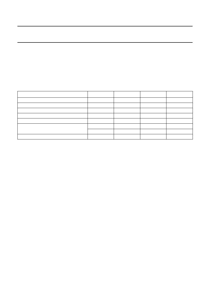
Table 1 gives an operational summary.
Table 1
Functionality of program pins
Notes
1. Where X = don’t care.
2. Not low means floating or high.
3. The NTC voltage has been to be less than 3.3 V, which indicates the presence of an NTC.
4. The NTC voltage is outside the window for NTC detection.
5. Vstb has to be floating or set to a battery regulating voltage in accordance with the specification.
FUNCTION
FCT
NTC
RFSH
Vstb
Inhibit
X(1)
low
Refresh
not low(2)
X(1)
low
not low
T/t detection
oating
note 3
not low
T/t and voltage peak detection
high
note 3
not low
Voltage peak detection
not low
note 4
not low
Trickle charge at standby
not low
X(1)
not low
high
not low
note 4
not low
Voltage regulation at standby
not low
note 3
not low
oating(5)
Supply block
The supply block delivers the following outputs:
A power-on reset pulse to reset all digital circuitry at
battery insertion or supply switch-on. After a general
reset the system will start fast charging the battery.
A 4.25 V stabilized voltage source (VS) is externally
available. This source can be used to set the thermistor
biasing, to initialize the programs, to supply the external
circuitry for battery voltage based charge indication and
to supply other external circuitry.
A 4.25 V bias voltage (Vsl) is available for use for more
indication LEDs. This output pin will be zero during the
initialization period at start-up, thus avoiding any
interference of the extra LEDs when initializing.
Charge control
The charge current is sensed via a low-ohmic resistor
(Rsense), see Fig.4. A positive voltage is created across
resistor Rb by means of a current source Iref which is set by
Rref in the event of fast charge and by an internal bias
current source in the event of top-off and trickle charge
(IIB), see Fig.1. The positive node of Rb will be regulated to
zero via error amplifier A1, which means that the voltage
across Rb and Rsense will be the same. The fast charge
current is defined by the following equation:
(1)
The output of amplifier A1 is available at the loop stability
pin LS, consequently the time constant of the current loop
can be set. When Vpeak (NiCd and NiMH) is applied, the
current sensing for the battery voltage will be reduced,
implying that the charge current will be regulated to zero
during:
(2)
Actually battery voltage sensing takes place in the last
oscillator cycle of this period.
I
fast
R
sense
×
R
b
I
ref
×
=
t
sense
2
10
POD
×
t
osc
×
=
相關(guān)PDF資料 |
PDF描述 |
|---|---|
| TEC3025 | High-Speed RISC Delay Modules |
| TEC3033 | High-Speed RISC Delay Modules |
| TEC3040 | High-Speed RISC Delay Modules |
| TEE310XBCC40M000000BBCA | TCXO, CLOCK, 40 MHz, CMOS OUTPUT |
| TEE310XBCC40M000000CADA | TCXO, CLOCK, 40 MHz, CMOS OUTPUT |
相關(guān)代理商/技術(shù)參數(shù) |
參數(shù)描述 |
|---|---|
| TEA1104 | 制造商:PHILIPS 制造商全稱:NXP Semiconductors 功能描述:Cost effective battery monitor and fast charge IC for NiCd and NiMH chargers |
| TEA1104/N2 | 制造商:NXP Semiconductors 功能描述: |
| TEA1104T | 制造商:PHILIPS 制造商全稱:NXP Semiconductors 功能描述:Cost effective battery monitor and fast charge IC for NiCd and NiMH chargers |
| TEA1104TD-T | 制造商:未知廠家 制造商全稱:未知廠家 功能描述:Battery Management |
| TEA1110 | 制造商:PHILIPS 制造商全稱:NXP Semiconductors 功能描述:Low voltage versatile telephone transmission circuit with dialler interface |
發(fā)布緊急采購,3分鐘左右您將得到回復(fù)。