- 您現(xiàn)在的位置:買(mǎi)賣(mài)IC網(wǎng) > PDF目錄383942 > TE28F320S3-120 (Intel Corp.) 16 Characters x 2 Lines, 5x7 Dot Matrix Character and Cursor PDF資料下載
參數(shù)資料
| 型號(hào): | TE28F320S3-120 |
| 廠商: | Intel Corp. |
| 英文描述: | 16 Characters x 2 Lines, 5x7 Dot Matrix Character and Cursor |
| 中文描述: | 字寬FlashFile⑩Memory系列 |
| 文件頁(yè)數(shù): | 14/52頁(yè) |
| 文件大小: | 1262K |
| 代理商: | TE28F320S3-120 |
第1頁(yè)第2頁(yè)第3頁(yè)第4頁(yè)第5頁(yè)第6頁(yè)第7頁(yè)第8頁(yè)第9頁(yè)第10頁(yè)第11頁(yè)第12頁(yè)第13頁(yè)當(dāng)前第14頁(yè)第15頁(yè)第16頁(yè)第17頁(yè)第18頁(yè)第19頁(yè)第20頁(yè)第21頁(yè)第22頁(yè)第23頁(yè)第24頁(yè)第25頁(yè)第26頁(yè)第27頁(yè)第28頁(yè)第29頁(yè)第30頁(yè)第31頁(yè)第32頁(yè)第33頁(yè)第34頁(yè)第35頁(yè)第36頁(yè)第37頁(yè)第38頁(yè)第39頁(yè)第40頁(yè)第41頁(yè)第42頁(yè)第43頁(yè)第44頁(yè)第45頁(yè)第46頁(yè)第47頁(yè)第48頁(yè)第49頁(yè)第50頁(yè)第51頁(yè)第52頁(yè)
28F160S3, 28F320S3
E
14
ADVANCE INFORMATION
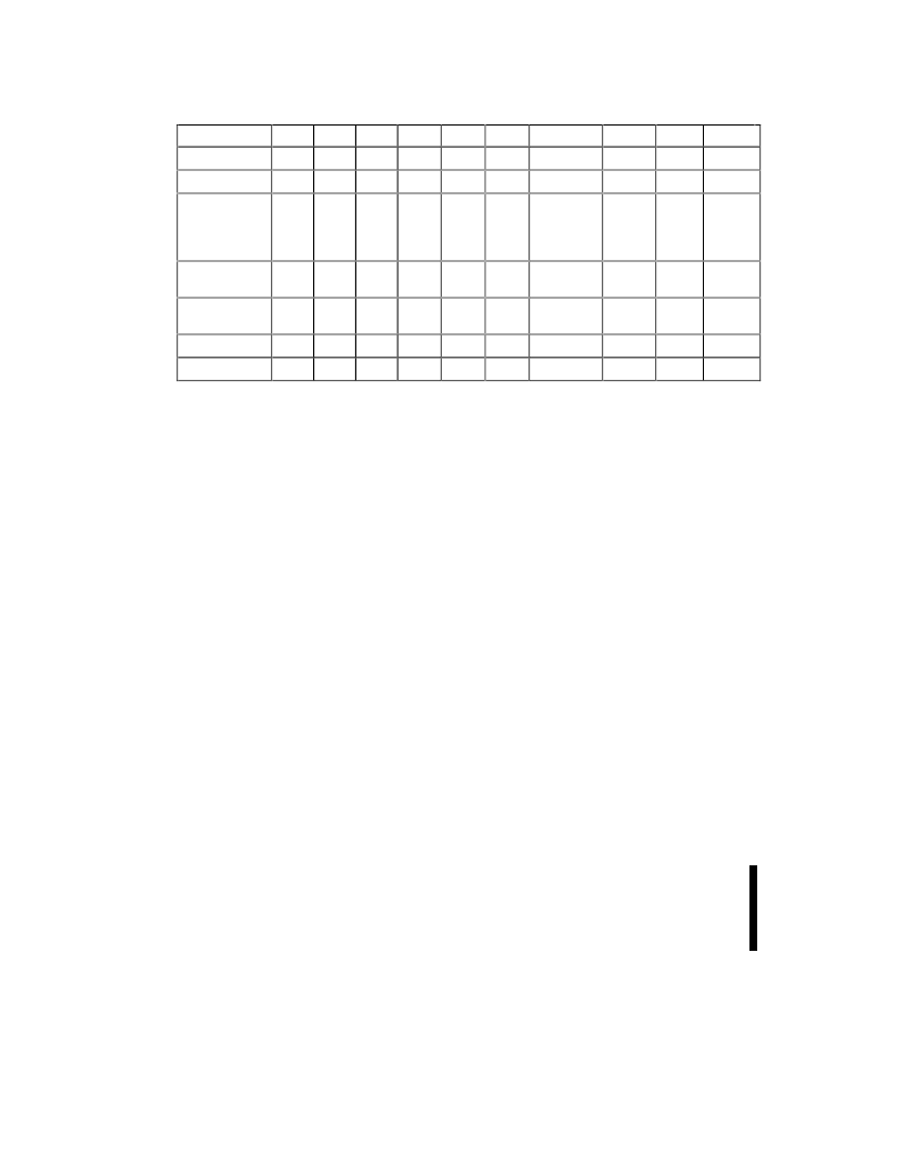
Table 2. Bus Operations
Mode
Notes
RP#
CE
0
#
CE
1
# OE#
(11)
WE#
(11)
Address
V
PP
DQ
(8)
STS
(3)
Read
1,2
V
IH
V
IL
V
IL
V
IL
V
IH
X
X
D
OUT
X
Output Disable
V
IH
V
IL
V
IL
V
IH
V
IH
X
X
High Z
X
Standby
V
IH
V
IL
V
IH
V
IH
V
IH
V
IL
V
IH
X
X
X
X
High Z
X
Reset/Power-
Down Mode
10
V
IL
X
X
X
X
X
X
High Z
High Z
(9)
Read Identifier
Codes
4
V
IH
V
IL
V
IL
V
IL
V
IH
See
Figure 6
X
D
OUT
High Z
(9)
Read Query
5
V
IH
V
IL
V
IL
V
IL
V
IH
See Table 6
X
D
OUT
High Z
(9)
Write
3,6,7
V
IH
V
IL
V
IL
V
IH
V
IL
X
V
PPH1/2
D
IN
X
NOTES:
1. Refer to Table 19. When V
PP
≤
V
PPLK
, memory contents can be read, but not altered.
2. X can be V
IL
or V
IH
for control and address input pins and V
PPLK
or V
PPH1/2
for V
PP
. See Table 19, for V
PPLK
and V
PPH1/2
voltages.
3. STS in level RY/BY# mode (default) is V
OL
when the WSM is executing internal block erase, programming, or lock-bit
configuration algorithms. It is V
OH
when the WSM is not busy, in block erase suspend mode (with programming inactive),
program suspend mode, or deep power-down mode.
4. See Section 4.3 for read identifier code data.
5. See Section 4.2 for read query data.
6. Command writes involving block erase, write, or lock-bit configuration are reliably executed when V
PP
= V
PPH1/2
and
V
CC
= V
CC1/2
(see Section 6.2).
7. Refer to Table 3 for valid D
IN
during a write operation.
8. DQ refers to DQ
0
–7
if BYTE# is low and DQ
0–15
if BYTE# is high.
9. High Z will be V
OH
with an external pull-up resistor.
10.
RP# at GND ± 0.2V ensures the lowest deep power-down current.
11. OE# = V
IL
and WE# = V
IL
concurrently is an undefined state and should not be attempted.
相關(guān)PDF資料 |
PDF描述 |
|---|---|
| TE28F160S3-120 | 16 Characters x 2 Lines, 5x7 Dot Matrix Character and Cursor |
| TE28F400B3T90 | 3 Volt Advanced Boot Block Flash Memory |
| TE28F004 | 3 Volt Advanced Boot Block Flash Memory |
| TE28F004B3T90 | 3 Volt Advanced Boot Block Flash Memory |
| TE28F640B3TC100 | 3 Volt Advanced Boot Block Flash Memory |
相關(guān)代理商/技術(shù)參數(shù) |
參數(shù)描述 |
|---|---|
| TE28F400B3 | 制造商:INTEL 制造商全稱(chēng):Intel Corporation 功能描述:SMART 3 ADVANCED BOOT BLOCK WORD-WIDE |
| TE28F400B3B110 | 制造商:INTEL 制造商全稱(chēng):Intel Corporation 功能描述:SMART 3 ADVANCED BOOT BLOCK 4-, 8-, 16-, 32-MBIT FLASH MEMORY FAMILY |
| TE28F400B3B120 | 制造商:INTEL 制造商全稱(chēng):Intel Corporation 功能描述:SMART 3 ADVANCED BOOT BLOCK WORD-WIDE |
| TE28F400B3-B120 | 制造商:INTEL 制造商全稱(chēng):Intel Corporation 功能描述:SMART 3 ADVANCED BOOT BLOCK WORD-WIDE |
| TE28F400B3B150 | 制造商:INTEL 制造商全稱(chēng):Intel Corporation 功能描述:SMART 3 ADVANCED BOOT BLOCK WORD-WIDE |
發(fā)布緊急采購(gòu),3分鐘左右您將得到回復(fù)。