- 您現(xiàn)在的位置:買賣IC網(wǎng) > PDF目錄383943 > TE28F320C3 (Intel Corp.) 3 Volt Intel Advanced+ Boot Block Flash Memory PDF資料下載
參數(shù)資料
| 型號(hào): | TE28F320C3 |
| 廠商: | Intel Corp. |
| 英文描述: | 3 Volt Intel Advanced+ Boot Block Flash Memory |
| 中文描述: | 3伏英特爾高級(jí)啟動(dòng)塊閃存 |
| 文件頁(yè)數(shù): | 12/58頁(yè) |
| 文件大?。?/td> | 920K |
| 代理商: | TE28F320C3 |
第1頁(yè)第2頁(yè)第3頁(yè)第4頁(yè)第5頁(yè)第6頁(yè)第7頁(yè)第8頁(yè)第9頁(yè)第10頁(yè)第11頁(yè)當(dāng)前第12頁(yè)第13頁(yè)第14頁(yè)第15頁(yè)第16頁(yè)第17頁(yè)第18頁(yè)第19頁(yè)第20頁(yè)第21頁(yè)第22頁(yè)第23頁(yè)第24頁(yè)第25頁(yè)第26頁(yè)第27頁(yè)第28頁(yè)第29頁(yè)第30頁(yè)第31頁(yè)第32頁(yè)第33頁(yè)第34頁(yè)第35頁(yè)第36頁(yè)第37頁(yè)第38頁(yè)第39頁(yè)第40頁(yè)第41頁(yè)第42頁(yè)第43頁(yè)第44頁(yè)第45頁(yè)第46頁(yè)第47頁(yè)第48頁(yè)第49頁(yè)第50頁(yè)第51頁(yè)第52頁(yè)第53頁(yè)第54頁(yè)第55頁(yè)第56頁(yè)第57頁(yè)第58頁(yè)
28F004/400B3, 28F008/800B3, 28F016/160B3, 28F320B3, 28F640B3
6
3UHOLPLQDU\
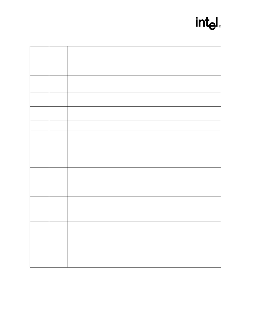
Table 2. 3 Volt Advanced Boot Block Pin Descriptions
Symbol
Type
Name and Function
A
0
–A
21
INPUT
ADDRESS INPUTS
for memory addresses. Addresses are internally latched during a program or
erase cycle.
28F004B3: A[0-18], 28F008B3: A[0-19], 28F016B3: A[0-20],
28F400B3: A[0-17], 28F800B3: A[0-18], 28F160B3: A[0-19],
28F320B3: A[0-20], 28F640B3: A[0-21]
DQ
0
–DQ
7
INPUT/
OUTPUT
DATA INPUTS/OUTPUTS:
Inputs array data on the second CE# and WE# cycle during a Program
command. Inputs commands to the Command User Interface when CE# and WE# are active. Data is
internally latched. Outputs array, identifier and status register data. The data pins float to tri-state when
the chip is de-selected or the outputs are disabled.
DQ
8
–
DQ
15
INPUT/
OUTPUT
DATA INPUTS/OUTPUTS:
Inputs array data on the second CE# and WE# cycle during a Program
command. Data is internally latched. Outputs array and identifier data. The data pins float to tri-state
when the chip is de-selected.
Not included on x8 products.
CE#
INPUT
CHIP ENABLE:
Activates the internal control logic, input buffers, decoders and sense amplifiers. CE#
is active low. CE# high de-selects the memory device and reduces power consumption to standby
levels.
OE#
INPUT
OUTPUT ENABLE:
Enables the device’s outputs through the data buffers during a read operation.
OE# is active low.
WE#
INPUT
WRITE ENABLE:
Controls writes to the Command Register and memory array. WE# is active low.
Addresses and data are latched on the rising edge of the second WE# pulse.
RP#
INPUT
RESET/DEEP POWER-DOWN:
Uses two voltage levels (V
IL
, V
IH
) to control reset/deep power-down
mode.
When RP# is at logic low, the device is in reset/deep power-down mode
, which drives the outputs
to High-Z, resets the Write State Machine, and minimizes current levels (I
CCD
).
When RP# is at logic high, the device is in standard operation
. When RP# transitions from logic-
low to logic-high, the device defaults to the read array mode.
WP#
INPUT
WRITE PROTECT:
Provides a method for locking and unlocking the two lockable parameter blocks.
When WP# is at logic low, the lockable blocks are locked
, preventing program and erase
operations to those blocks. If a program or erase operation is attempted on a locked block, SR.1 and
either SR.4 [program] or SR.5 [erase] will be set to indicate the operation failed.
When WP# is at logic high, the lockable blocks are unlocked
and can be programmed or erased.
See
Section 3.3
for details on write protection.
V
CCQ
INPUT
OUTPUT V
CC
:
Enables all outputs to be driven to 1.8 V – 2.5 V while the V
CC
is at 2.7 V–3.3 V. If the
V
CC
is regulated to 2.7 V–2.85 V, V
CCQ
can be driven at 1.65 V–2.5 V to achieve lowest power
operation (see
Section 4.4
)
.
This input may be tied directly to V
CC
(2.7 V–3.6 V).
V
CC
DEVICE POWER SUPPLY:
2.7 V–3.6 V
V
PP
PROGRAM/ERASE POWER SUPPLY:
Supplies power for program and erase operations. V
PP
may
be the same as V
CC
(2.7 V–3.6 V) for single supply voltage operation. For fast programming at
manufacturing, 11.4 V–12.6 V may be supplied to V
PP
. This pin cannot be left floating. Applying
11.4 V–12.6 V to V
PP
can only be done for a maximum of 1000 cycles on the main blocks and 2500
cycles on the parameter blocks.
V
PP
may be connected to 12 V for a total of 80 hours maximum (see
Section 3.4
for details).
V
PP
< V
PPLK
protects memory contents against inadvertent or unintended program and erase
commands.
GND
GROUND:
For all internal circuitry. All ground inputs
must
be connected.
NC
NO CONNECT:
Pin may be driven or left floating.
相關(guān)PDF資料 |
PDF描述 |
|---|---|
| TE28F004B3B110 | 3 Volt Advanced Boot Block Flash Memory |
| TE28F004B3B90 | 3 Volt Advanced Boot Block Flash Memory |
| TE28F320B3TA100 | 3 Volt Advanced Boot Block Flash Memory |
| TE28F004BX-B80 | Series RR3112 round rocker switches have an ergonomic feel and multiple circuit options |
| TE28F004BX-T80 | Series RR3130 round rocker switches have an ergonomic euro design and panel mounting |
相關(guān)代理商/技術(shù)參數(shù) |
參數(shù)描述 |
|---|---|
| TE28F320C3B110 | 制造商:INTEL 制造商全稱:Intel Corporation 功能描述:3 VOLT ADVANCED+ BOOT BLOCK 8-, 16-, 32-MBIT FLASH MEMORY FAMILY |
| TE28F320C3B90 | 制造商:INTEL 制造商全稱:Intel Corporation 功能描述:3 VOLT ADVANCED+ BOOT BLOCK 8-, 16-, 32-MBIT FLASH MEMORY FAMILY |
| TE28F320C3BA100 | 制造商:NA 功能描述:NOR Flash, 2M x 16, 48 Pin, Plastic, TSSOP |
| TE28F320C3BA110 | 制造商:INTEL 制造商全稱:Intel Corporation 功能描述:Advanced+ Boot Block Flash Memory (C3) |
| TE28F320C3BA70 | 制造商:INTEL 制造商全稱:Intel Corporation 功能描述:Advanced+ Boot Block Flash Memory (C3) |
發(fā)布緊急采購(gòu),3分鐘左右您將得到回復(fù)。