- 您現(xiàn)在的位置:買賣IC網(wǎng) > PDF目錄383943 > TE28F004B3B110 (INTEL CORP) 3 Volt Advanced Boot Block Flash Memory PDF資料下載
參數(shù)資料
| 型號: | TE28F004B3B110 |
| 廠商: | INTEL CORP |
| 元件分類: | DRAM |
| 英文描述: | 3 Volt Advanced Boot Block Flash Memory |
| 中文描述: | 512K X 8 FLASH 3V PROM, 110 ns, PDSO40 |
| 封裝: | 10 X 20 MM, TSOP-40 |
| 文件頁數(shù): | 16/58頁 |
| 文件大?。?/td> | 920K |
| 代理商: | TE28F004B3B110 |
第1頁第2頁第3頁第4頁第5頁第6頁第7頁第8頁第9頁第10頁第11頁第12頁第13頁第14頁第15頁當前第16頁第17頁第18頁第19頁第20頁第21頁第22頁第23頁第24頁第25頁第26頁第27頁第28頁第29頁第30頁第31頁第32頁第33頁第34頁第35頁第36頁第37頁第38頁第39頁第40頁第41頁第42頁第43頁第44頁第45頁第46頁第47頁第48頁第49頁第50頁第51頁第52頁第53頁第54頁第55頁第56頁第57頁第58頁
28F004/400B3, 28F008/800B3, 28F016/160B3, 28F320B3, 28F640B3
10
3UHOLPLQDU\
When the device is in read array mode, four control signals control data output:
WE# must be logic high (V
IH
)
CE# must be logic low (V
IL
)
OE# must be logic low (V
IL
)
RP# must be logic high (V
IH
)
In addition, the address of the desired location must be applied to the address pins. If the device is
not in read array mode, as would be the case after a program or erase operation, the Read Array
command (FFH) must be written to the CUI before array reads can take place.
NOTE:
See
Appendix A
for mode transition information.
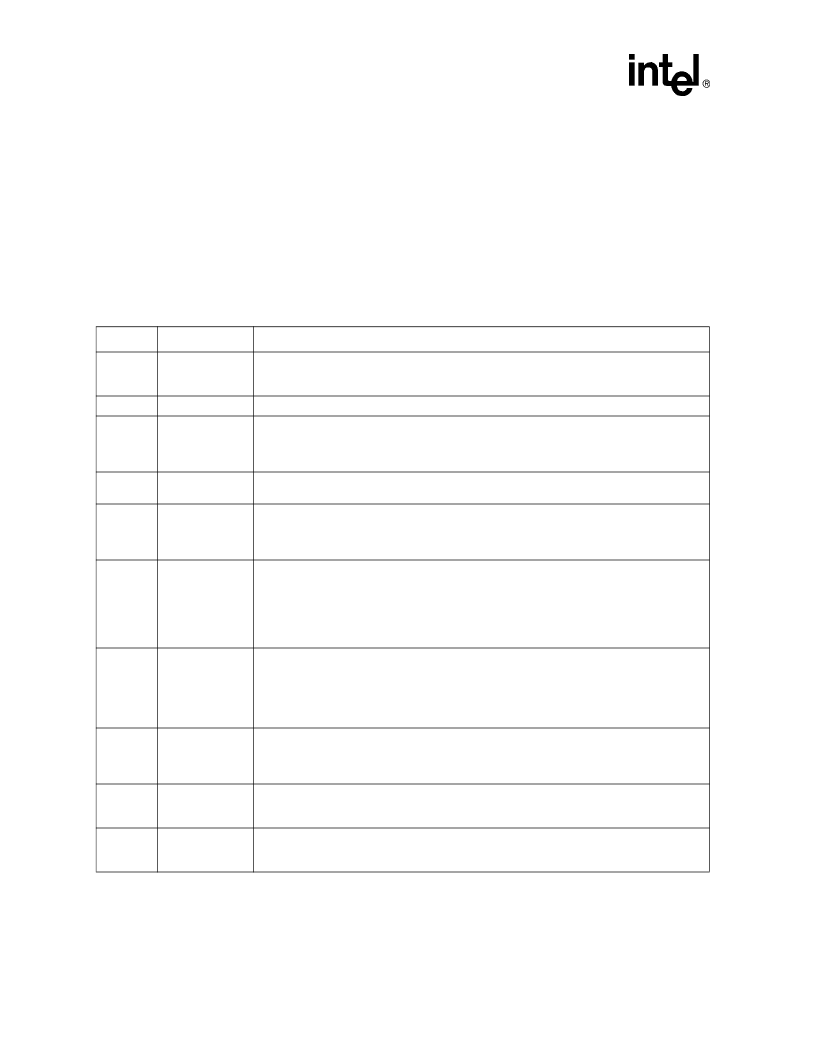
Table 4. Command Codes and Descriptions
Code
Device Mode
Description
00, 01,
60, 2F,
C0, 98
Invalid/
Reserved
Unassigned commands that should not be used. Intel reserves the right to redefine these
codes for future functions.
FF
Read Array
Places the device in read array mode, such that array data will be output on the data pins.
40
Program Set-Up
This is a two-cycle command. The first cycle prepares the CUI for a program operation. The
second cycle latches addresses and data information and initiates the WSM to execute the
Program algorithm. The flash outputs status register data when CE# or OE# is toggled. A Read
Array command is required after programming to read array data. See
Section 3.2.4
.
10
Alternate
Program Set-Up
(See 40H/Program Set-Up)
20
Erase Set-Up
Prepares the CUI for the Erase Confirm command. If the next command is not an Erase
Confirm command, then the CUI will (a) set both SR.4 and SR.5 of the status register to a “1,”
(b) place the device into the read status register mode, and (c) wait for another command. See
Section 3.2.5
.
D0
Erase Confirm
Program / Erase
Resume
If the previous command was an Erase Set-Up command, then the CUI will close the address
and data latches, and begin erasing the block indicated on the address pins. During erase, the
device will only respond to the Read Status Register and Erase Suspend commands. The
device will output status register data when CE# or OE# is toggled.
If a program or erase operation was previously suspended, this command will resume that
operation
B0
Program / Erase
Suspend
Issuing this command will begin to suspend the currently executing program/erase operation.
The status register will indicate when the operation has been successfully suspended by
setting either the program suspend (SR.2) or erase suspend (SR.6) and the WSM status bit
(SR.7) to a “1” (ready). The WSM will continue to idle in the SUSPEND state, regardless of the
state of all input control pins except RP#, which will immediately shut down the WSM and the
remainder of the chip if it is driven to V
IL
. See
Section 3.2.4.1
and
Section 3.2.4.1
.
70
Read Status
Register
This command places the device into read status register mode. Reading the device will output
the contents of the status register, regardless of the address presented to the device. The
device automatically enters this mode after a program or erase operation has been initiated.
See
Section 3.2.3
.
50
Clear Status
Register
The WSM can set the block lock status (SR.1) , V
status (SR.3), program status (SR.4), and
erase status (SR.5) bits in the status register to “1,” but it cannot clear them to “0.” Issuing this
command clears those bits to “0.”
90
Read Identifier
Puts the device into the intelligent identifier read mode, so that reading the device will output
the manufacturer and device codes (A
0
= 0 for manufacturer, A
0
= 1 for device, all other
address inputs must be 0). See Section
Section 3.2.2
.
相關PDF資料 |
PDF描述 |
|---|---|
| TE28F004B3B90 | 3 Volt Advanced Boot Block Flash Memory |
| TE28F320B3TA100 | 3 Volt Advanced Boot Block Flash Memory |
| TE28F004BX-B80 | Series RR3112 round rocker switches have an ergonomic feel and multiple circuit options |
| TE28F004BX-T80 | Series RR3130 round rocker switches have an ergonomic euro design and panel mounting |
| TE28F004BVB80 | 4-MBIT (256K X 16, 512K X 8)SmartVoltage BOOT BLOCK FLASH MEMORY FAMILY |
相關代理商/技術參數(shù) |
參數(shù)描述 |
|---|---|
| TE28F004B3B90 | 制造商:INTEL 制造商全稱:Intel Corporation 功能描述:3 Volt Advanced Boot Block Flash Memory |
| TE28F004B3T110 | 制造商:INTEL 制造商全稱:Intel Corporation 功能描述:3 Volt Advanced Boot Block Flash Memory |
| TE28F004B3T90 | 制造商:INTEL 制造商全稱:Intel Corporation 功能描述:3 Volt Advanced Boot Block Flash Memory |
| TE28F004B5B80 | 制造商:Intel 功能描述: |
| TE28F004BEB120 | 制造商:INTEL 制造商全稱:Intel Corporation 功能描述:4-MBIT (256K X 16, 512K X 8)SmartVoltage BOOT BLOCK FLASH MEMORY FAMILY |
發(fā)布緊急采購,3分鐘左右您將得到回復。