- 您現(xiàn)在的位置:買賣IC網(wǎng) > PDF目錄196353 > TCA8418EYFPR (TEXAS INSTRUMENTS INC) SPECIALTY ANALOG CIRCUIT, BGA25 PDF資料下載
參數(shù)資料
| 型號(hào): | TCA8418EYFPR |
| 廠商: | TEXAS INSTRUMENTS INC |
| 元件分類: | 模擬信號(hào)調(diào)理 |
| 英文描述: | SPECIALTY ANALOG CIRCUIT, BGA25 |
| 封裝: | 2 X 2 MM, 0.40 MM PITCH, DSBGA-25 |
| 文件頁(yè)數(shù): | 3/31頁(yè) |
| 文件大?。?/td> | 400K |
| 代理商: | TCA8418EYFPR |
第1頁(yè)第2頁(yè)當(dāng)前第3頁(yè)第4頁(yè)第5頁(yè)第6頁(yè)第7頁(yè)第8頁(yè)第9頁(yè)第10頁(yè)第11頁(yè)第12頁(yè)第13頁(yè)第14頁(yè)第15頁(yè)第16頁(yè)第17頁(yè)第18頁(yè)第19頁(yè)第20頁(yè)第21頁(yè)第22頁(yè)第23頁(yè)第24頁(yè)第25頁(yè)第26頁(yè)第27頁(yè)第28頁(yè)第29頁(yè)第30頁(yè)第31頁(yè)
SDA
SCL
S
P
StartCondition
StopCondition
SDA
SCL
DataLine
Change
www.ti.com
SCPS222B – MAY 2010 – REVISED SEPTEMBER 2010
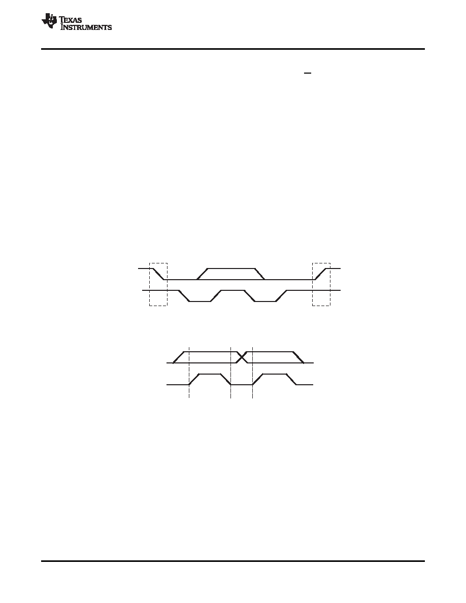
I2C communication with this device is initiated by a master sending a Start condition, a high-to-low transition on
the SDA input/output, while the SCL input is high (see Figure 5). After the Start condition, the device address
byte is sent, most significant bit (MSB) first, including the data direction bit (R/W).
After receiving the valid address byte, this device responds with an acknowledge (ACK), a low on the SDA
input/output during the high of the ACK-related clock pulse. The address (ADDR) input of the slave device must
not be changed between the Start and the Stop conditions.
On the I2C bus, only one data bit is transferred during each clock pulse. The data on the SDA line must remain
stable during the high pulse of the clock period, as changes in the data line at this time are interpreted as control
commands (Start or Stop) (see Figure 6).
A Stop condition, a low-to-high transition on the SDA input/output while the SCL input is high, is sent by the
master (see Figure 5).
Any number of data bytes can be transferred from the transmitter to receiver between the Start and the Stop
conditions. Each byte of eight bits is followed by one ACK bit. The transmitter must release the SDA line before
the receiver can send an ACK bit. The device that acknowledges must pull down the SDA line during the ACK
clock pulse, so that the SDA line is stable low during the high pulse of the ACK-related clock period (see
Figure 7). When a slave receiver is addressed, it must generate an ACK after each byte is received. Similarly,
the master must generate an ACK after each byte that it receives from the slave transmitter. Setup and hold
times must be met to ensure proper operation.
A master receiver signals an end of data to the slave transmitter by not generating an acknowledge (NACK) after
the last byte has been clocked out of the slave. This is done by the master receiver by holding the SDA line high.
In this event, the transmitter must release the data line to enable the master to generate a Stop condition.
Figure 5. Definition of Start and Stop Conditions
Figure 6. Bit Transfer
Copyright 2010, Texas Instruments Incorporated
11
Product Folder Link(s): TCA8418E
相關(guān)PDF資料 |
PDF描述 |
|---|---|
| TCD2253D | SPECIALTY ANALOG CIRCUIT, CDIP22 |
| TCD4027036BC015000-12.75M | TCXO, CLIPPED SINE OUTPUT, 12.75 MHz |
| TCD4029055DK015000-10M | TCXO, CLIPPED SINE OUTPUT, 10 MHz |
| TCD4027036EH015000-12.75M | TCXO, CLIPPED SINE OUTPUT, 12.75 MHz |
| TCD4027036FG015000-12.75M | TCXO, CLIPPED SINE OUTPUT, 12.75 MHz |
相關(guān)代理商/技術(shù)參數(shù) |
參數(shù)描述 |
|---|---|
| TCA8418EYFPR | 制造商:Texas Instruments 功能描述:IC I2C CONTROLLED KEYPAD SCAN 3.6V 25 |
| TCA8418RTWR | 功能描述:I2C 接口集成電路 Low-Vltg 16B I2C & SMBus I/O Expander RoHS:否 制造商:NXP Semiconductors 電源電壓-最大:5.5 V 電源電壓-最小:2.3 V 最大工作頻率:400 KHz 最大工作溫度:+ 85 C 封裝 / 箱體:TSSOP-16 |
| TCA8418YFPR | 制造商:TI 制造商全稱:Texas Instruments 功能描述:I2C CONTROLLED KEYPAD SCAN IC WITH INTEGRATED ESD PROTECTION |
| TCA8424 | 制造商:TI 制造商全稱:Texas Instruments 功能描述:Check for Samples: TCA8424 |
| TCA8424EVM-038 | 功能描述:界面開發(fā)工具 TCA8424 EVAL MOD RoHS:否 制造商:Bourns 產(chǎn)品:Evaluation Boards 類型:RS-485 工具用于評(píng)估:ADM3485E 接口類型:RS-485 工作電源電壓:3.3 V |
發(fā)布緊急采購(gòu),3分鐘左右您將得到回復(fù)。