- 您現(xiàn)在的位置:買賣IC網(wǎng) > PDF目錄383868 > SY89295U (Micrel Semiconductor,Inc.) 2.5V / 3.3V 1.5 GHZ PRECISION LVPECL PROGRAMMABLE DELAY PDF資料下載
參數(shù)資料
| 型號(hào): | SY89295U |
| 廠商: | Micrel Semiconductor,Inc. |
| 英文描述: | 2.5V / 3.3V 1.5 GHZ PRECISION LVPECL PROGRAMMABLE DELAY |
| 中文描述: | 為2.5V / 3.3V的1.5 GHz的精密可編程延遲的LVPECL |
| 文件頁數(shù): | 7/15頁 |
| 文件大?。?/td> | 169K |
| 代理商: | SY89295U |
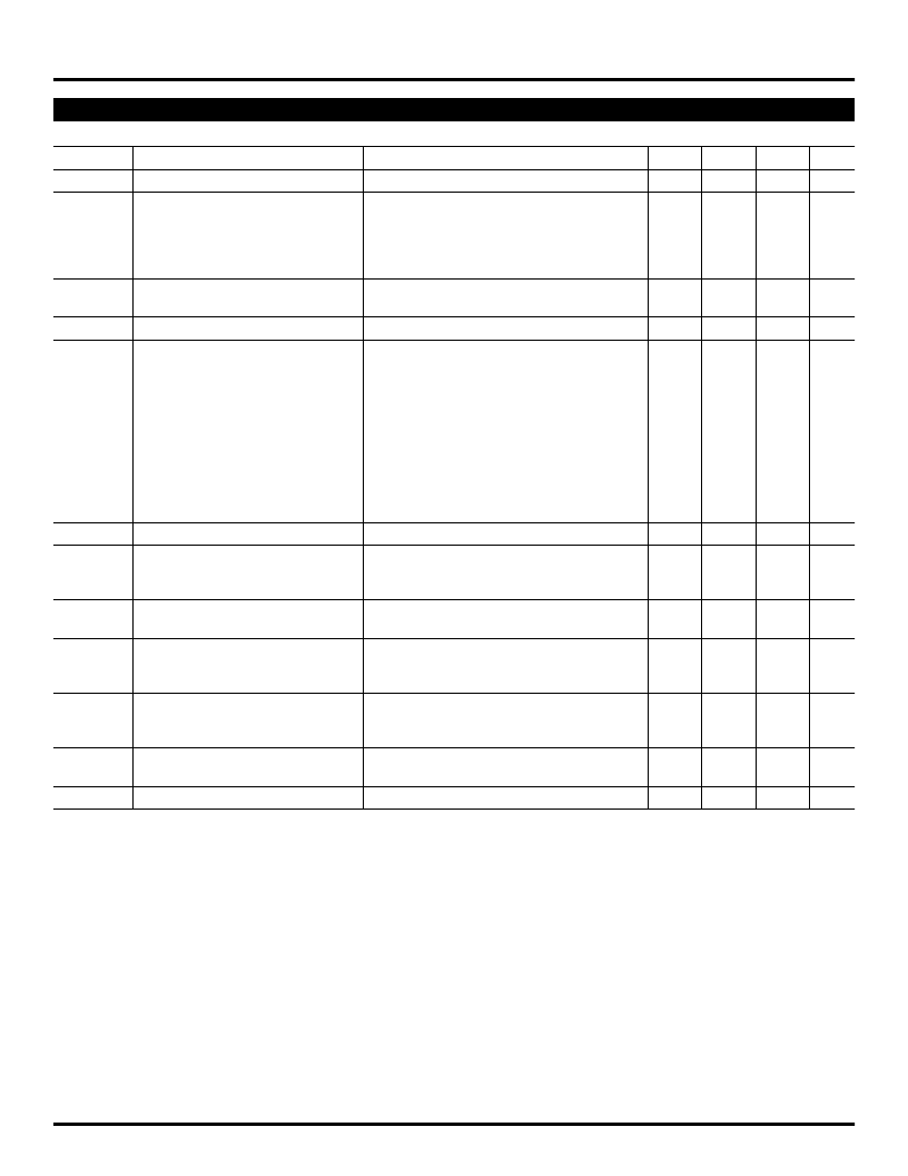
7
Precision Edge
SY89295U
Micrel
M9999-031604
hbwhelp@micrel.com or (408) 955-1690
T
A
=
–
40
°
C to +85
°
C; unless otherwise stated.
Symbol
Parameter
f
MAX
Maximum Operating Frequency
t
pd
Propagation Delay
Condition
Clock V
OUT
≥
400mV
Min
1.5
Typ
Max
Units
GHz
IN to Q; D[0
–
10]=0
IN to Q; D[0
–
10]=1023
/EN to Q: D[0
–
10]=0
D10 to CASCADE
3200
11500
3400
350
4200
14800
4400
670
ps
ps
ps
ps
t
RANGE
Programmable Range
t
pd
(max)
–
t
pd
(min)
8300
ps
t
SKEW
t
Duty Cycle Skew
Note 8
25
ps
Step Delay
D0 High
D1 High
D2 High
D3 High
D4 High
D5 High
D6 High
D7 High
D8 High
D9 High
D0-D9 High
10
15
35
70
145
290
575
1150
2300
4610
9220
ps
ps
ps
ps
ps
ps
ps
ps
ps
ps
ps
INL
Integral Non-Linearity
Note 9
–
10
+10
%LSB
t
S
Setup Time
D to LEN
D to IN
/EN to IN
200
350
300
ps
ps
ps
Note 10
Note 11
t
H
Hold Time
LEN to D
IN to /EN
200
400
ps
ps
Note 12
t
R
Release Time
/EN to IN
500
500
450
ps
ps
ps
SETMAX to LEN
SETMIN to LEN
t
JITTER
Cycle-to-Cycle Jitter
Total Jitter
Random Jitter
Note 13
Note 14
Note 15
20% to 80% (Q)
20% to 80% (CASCADE)
2
10
1
ps
rms
ps
p-p
ps
rms
ps
ps
t
r
, t
f
Output Rise/Fall Time
50
90
85
160
300
Duty Cycle
45
55
%
Notes:
7. High frequency AC electricals are guaranteed by design and characterization.
8. Duty cycle skew guaranteed only for differential operation measured from the cross point of the input to the crosspoint of the output.
9. INL (Integral Non-Linearity) is defined from its corresponding point on the ideal delay versus D[9:0] curve as the deviation from its ideal delay. The
maximum difference is the INL. Theoretical Ideal Linearity (TIL) = (measured maximum delay
–
measured minimum delay)
÷
1024. INL = measured
delay
–
measured minimum delay + (step number
×
TIL).
10. This setup time defines the amount of time prior to the input signal. The delay tap of the device must be set.
11. This setup time defines the amount of the time that /EN must be asserted prior to the next transition of IN, /IN to prevent an output response greater
than
±
75mV to the IN, /IN transition.
12. Hold time is the minimum time that /EN must remain asserted after a negative going IN or a positive going /IN to prevent an output response greater
than
±
75mV to the IN, /IN transition.
13. Cycle-to-cycle jitter definition: The variation of periods between adjacent cycles over a random sample of adjacent cycle pairs.
T
jitter_cc
= T
n
–
T
n
+1, where T is the time between rising edges of the output signal.
14. Total jitter definition: With an ideal clock input, no more than one output edge in 10
12
output edges will deviate by more than the specified peak-to-
peak jitter value.
15. Random jitter definition: Jitter that is characterized by a Gaussian distribution, unbounded and is quantified by its standard deviation and mean.
Random jitter is measured with a K28.7 comma defect pattern, measured at 1.5Gbps.
AC ELECTRICAL CHARACTERISTICS
(7)
相關(guān)PDF資料 |
PDF描述 |
|---|---|
| SY89306 | 3.3V / 5V 2.5 GHZ PECL/ECL DIFFERENTIAL RECEIVER/BUFFER |
| SY89306V | 3.3V / 5V 2.5 GHZ PECL/ECL DIFFERENTIAL RECEIVER/BUFFER |
| SY89306VMGTR | 3.3V / 5V 2.5 GHZ PECL/ECL DIFFERENTIAL RECEIVER/BUFFER |
| SY89316V | 3.3V / 5V 2.5 GHZ PECL/ECL DIFFERENTIAL RECEIVER/BUFFER |
| SY89316VMGTR | 3.3V / 5V 2.5 GHZ PECL/ECL DIFFERENTIAL RECEIVER/BUFFER |
相關(guān)代理商/技術(shù)參數(shù) |
參數(shù)描述 |
|---|---|
| SY89295U_06 | 制造商:MICREL 制造商全稱:Micrel Semiconductor 功能描述:2.5V/3.3V 1.5GHz PRECISION LVPECL PROGRAMMABLE DELAY |
| SY89295U_11 | 制造商:MICREL 制造商全稱:Micrel Semiconductor 功能描述:2.5V/3.3V 1.5GHz Precision LVPECL |
| SY89295U-EVAL | 制造商:Micrel Inc 功能描述:2.5V/3.3V PECL DELAY LINE - EV |
| SY89295UMG | 功能描述:延遲線/計(jì)時(shí)元素 2.5V/3.3V PECL Delay Line (I Temp, Green) RoHS:否 制造商:Micrel 功能:Active Programmable Delay Line 傳播延遲時(shí)間:1000 ps 工作溫度范圍: 封裝 / 箱體:QFN-24 封裝:Tube |
| SY89295UMG TR | 功能描述:延遲線/計(jì)時(shí)元素 2.5V/3.3V PECL Delay Line (I Temp, Green) RoHS:否 制造商:Micrel 功能:Active Programmable Delay Line 傳播延遲時(shí)間:1000 ps 工作溫度范圍: 封裝 / 箱體:QFN-24 封裝:Tube |
發(fā)布緊急采購,3分鐘左右您將得到回復(fù)。