- 您現(xiàn)在的位置:買賣IC網(wǎng) > PDF目錄383868 > SY89295U (Micrel Semiconductor,Inc.) 2.5V / 3.3V 1.5 GHZ PRECISION LVPECL PROGRAMMABLE DELAY PDF資料下載
參數(shù)資料
| 型號: | SY89295U |
| 廠商: | Micrel Semiconductor,Inc. |
| 英文描述: | 2.5V / 3.3V 1.5 GHZ PRECISION LVPECL PROGRAMMABLE DELAY |
| 中文描述: | 為2.5V / 3.3V的1.5 GHz的精密可編程延遲的LVPECL |
| 文件頁數(shù): | 5/15頁 |
| 文件大小: | 169K |
| 代理商: | SY89295U |
5
Precision Edge
SY89295U
Micrel
M9999-0316
hbwhelp@micrel.com or (408) 955-1690
Absolute Maximum Ratings
(1)
Supply Voltage (V
CC
) ..................................
–
0.5V to +4.0V
Input Voltage (V
IN
) .........................................
–
0.5V to V
CC
LVPECL Output Current (I
OUT
)
Continuous .........................................................50mA
Surge................................................................100mA
Lead Temperature (soldering, 10 sec.) ................... +220
°
C
Storage Temperature Range (T
S
)............
–
65
°
C to +150
°
C
Operating Ratings
(2)
Supply Voltage (V
CC
) .............................. +2.375V to +3.6V
Ambient Temperature (T
A
).........................
–
40
°
C to +85
°
C
Package Thermal Resistance
(3)
MLF
(θ
JA
)
Still-Air .............................................................35
°
C/W
MLF
(ψ
JB
)
Junction-to-Board ............................................28
°
C/W
TQFP
(θ
JA
)
Still-Air .............................................................28
°
C/W
TQFP
(ψ
JB
)
Junction-to-Board ............................................20
°
C/W
T
A
=
–
40
°
C to 85
°
C, unless otherwise stated.
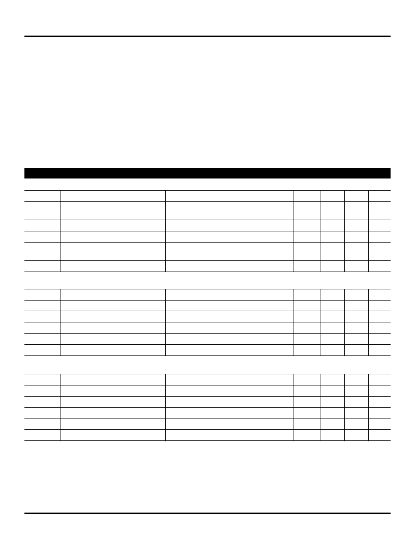
Symbol
Parameter
Condition
Min
Typ
Max
Units
V
CC
Power Supply
V
CC
= 2.5V
V
CC
= 3.3V
No load, max V
CC
See Figure 1a.
2.375
3
2.5
3.3
2.625
3.6
V
V
I
EE
V
IN
V
DIFF_IN
Power Supply Current
220
mA
Input Voltage Swing (IN, /IN)
150
1200
mV
Differential Input Voltage
Swing (IN, /IN)
See Figure 1b.
300
2400
mV
V
IHCMR
Input High Common Mode Range
IN, I
NB
V
EE
+1.2
V
CC
V
DC ELECTRICAL CHARACTERISTICS
(4)
V
CC
= 3.3V, T
A
=
–
40
°
C to 85
°
C, unless otherwise stated.
Symbol
Parameter
Condition
Min
Typ
Max
Units
V
IH
V
IL
V
BB
V
EF
V
CF
Input High Voltage (IN, /IN)
2.075
2.420
V
Input Low High Voltage (IN, /IN)
1.355
1.675
V
Output Voltage Reference
Ground Reference
1.325
1.425
1.525
V
Mode Connection
Ground Reference
1.20
1.30
1.4
V
Input Select Voltage
1.55
1.65
1.75
V
V
CC
= 2.5V, T
A
=
–
40
°
C to 85
°
C, unless otherwise stated.
Symbol
Parameter
Condition
Min
Typ
Max
Units
V
IH
V
IL
V
BB
V
EF
V
CF
Input High Voltage (IN, /IN)
2.075
2.42
V
Input Low High Voltage (IN, /IN)
1.355
1.675
V
Output Voltage Reference
Ground Reference
1.325
1.425
1.525
V
Mode Connection
Ground Reference
1.20
1.30
1.40
V
Input Select Voltage
1.15
1.25
1.35
V
Notes:
1. Permanent device damage may occur if the ratings in the
“
Absolute Maximum Ratings
”
section are exceeded. This is a stress rating only and
functional operation is not implied at conditions other than those detailed in the operational sections of this data sheet. Exposure to absolute
maximum ratings for extended periods may affect device reliability.
2. The data sheet limits are not guaranteed if the device is operated beyond the operating ratings.
3. Thermal performance on MLF
packages assumes exposed pad is soldered (or equivalent) to the device most negative potential (GND).
4. The circuit is designed to meet the DC specifications shown in the table above after thermal equilibrium has been established. Input and output
parameters vary 1:1 with V
CC
.
相關(guān)PDF資料 |
PDF描述 |
|---|---|
| SY89306 | 3.3V / 5V 2.5 GHZ PECL/ECL DIFFERENTIAL RECEIVER/BUFFER |
| SY89306V | 3.3V / 5V 2.5 GHZ PECL/ECL DIFFERENTIAL RECEIVER/BUFFER |
| SY89306VMGTR | 3.3V / 5V 2.5 GHZ PECL/ECL DIFFERENTIAL RECEIVER/BUFFER |
| SY89316V | 3.3V / 5V 2.5 GHZ PECL/ECL DIFFERENTIAL RECEIVER/BUFFER |
| SY89316VMGTR | 3.3V / 5V 2.5 GHZ PECL/ECL DIFFERENTIAL RECEIVER/BUFFER |
相關(guān)代理商/技術(shù)參數(shù) |
參數(shù)描述 |
|---|---|
| SY89295U_06 | 制造商:MICREL 制造商全稱:Micrel Semiconductor 功能描述:2.5V/3.3V 1.5GHz PRECISION LVPECL PROGRAMMABLE DELAY |
| SY89295U_11 | 制造商:MICREL 制造商全稱:Micrel Semiconductor 功能描述:2.5V/3.3V 1.5GHz Precision LVPECL |
| SY89295U-EVAL | 制造商:Micrel Inc 功能描述:2.5V/3.3V PECL DELAY LINE - EV |
| SY89295UMG | 功能描述:延遲線/計(jì)時元素 2.5V/3.3V PECL Delay Line (I Temp, Green) RoHS:否 制造商:Micrel 功能:Active Programmable Delay Line 傳播延遲時間:1000 ps 工作溫度范圍: 封裝 / 箱體:QFN-24 封裝:Tube |
| SY89295UMG TR | 功能描述:延遲線/計(jì)時元素 2.5V/3.3V PECL Delay Line (I Temp, Green) RoHS:否 制造商:Micrel 功能:Active Programmable Delay Line 傳播延遲時間:1000 ps 工作溫度范圍: 封裝 / 箱體:QFN-24 封裝:Tube |
發(fā)布緊急采購,3分鐘左右您將得到回復(fù)。