- 您現(xiàn)在的位置:買(mǎi)賣(mài)IC網(wǎng) > PDF目錄98143 > ST6242BQ1/XXX (STMICROELECTRONICS) 8-BIT, MROM, 8 MHz, MICROCONTROLLER, PQFP64 PDF資料下載
參數(shù)資料
| 型號(hào): | ST6242BQ1/XXX |
| 廠商: | STMICROELECTRONICS |
| 元件分類: | 微控制器/微處理器 |
| 英文描述: | 8-BIT, MROM, 8 MHz, MICROCONTROLLER, PQFP64 |
| 封裝: | PLASTIC, QFP-64 |
| 文件頁(yè)數(shù): | 25/69頁(yè) |
| 文件大?。?/td> | 1846K |
| 代理商: | ST6242BQ1/XXX |
第1頁(yè)第2頁(yè)第3頁(yè)第4頁(yè)第5頁(yè)第6頁(yè)第7頁(yè)第8頁(yè)第9頁(yè)第10頁(yè)第11頁(yè)第12頁(yè)第13頁(yè)第14頁(yè)第15頁(yè)第16頁(yè)第17頁(yè)第18頁(yè)第19頁(yè)第20頁(yè)第21頁(yè)第22頁(yè)第23頁(yè)第24頁(yè)當(dāng)前第25頁(yè)第26頁(yè)第27頁(yè)第28頁(yè)第29頁(yè)第30頁(yè)第31頁(yè)第32頁(yè)第33頁(yè)第34頁(yè)第35頁(yè)第36頁(yè)第37頁(yè)第38頁(yè)第39頁(yè)第40頁(yè)第41頁(yè)第42頁(yè)第43頁(yè)第44頁(yè)第45頁(yè)第46頁(yè)第47頁(yè)第48頁(yè)第49頁(yè)第50頁(yè)第51頁(yè)第52頁(yè)第53頁(yè)第54頁(yè)第55頁(yè)第56頁(yè)第57頁(yè)第58頁(yè)第59頁(yè)第60頁(yè)第61頁(yè)第62頁(yè)第63頁(yè)第64頁(yè)第65頁(yè)第66頁(yè)第67頁(yè)第68頁(yè)第69頁(yè)

Obsolete
Product(s)
- Obsolete
Product(s)
Obsolete
Product(s)
- Obsolete
Product(s)
31/69
ST62T42B/E42B
4 ON-CHIP PERIPHERALS
4.1 I/O PORTS
The MCU features Input/Output lines which may
be individually programmed as any of the following
input or output configurations:
– Input without pull-up or interrupt
– Input with pull-up and interrupt
– Input with pull-up, but without interrupt
– Analog input
– Push-pull output
– Open drain output
The lines are organised as bytewise Ports.
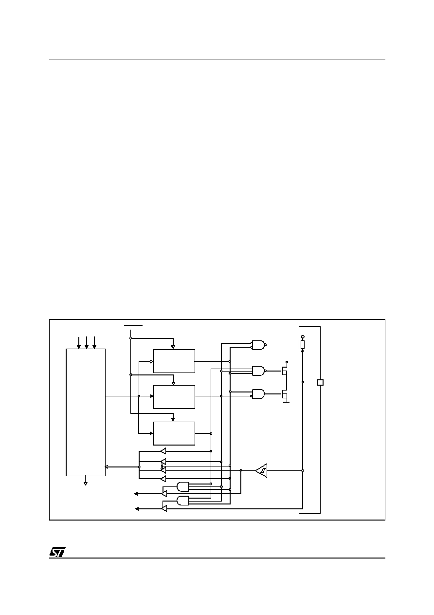
Each port is associated with 3 registers in Data
space. Each bit of these registers is associated
with a particular line (for instance, bits 0 of Port A
Data, Direction and Option registers are associat-
ed with the PA0 line of Port A).
The DATA registers (DRx), are used to read the
voltage level values of the lines which have been
configured as inputs, or to write the logic value of
the signal to be output on the lines configured as
outputs. The port data registers can be read to get
the effective logic levels of the pins, but they can
be also written by user software, in conjunction
with the related option registers, to select the dif-
ferent input mode options.
Single-bit operations on I/O registers are possible
but care is necessary because reading in input
mode is done from I/O pins while writing will direct-
ly affect the Port data register causing an unde-
sired change of the input configuration.
The Data Direction registers (DDRx) allow the
data direction (input or output) of each pin to be
set.
The Option registers (ORx) are used to select the
different port options available both in input and in
output mode.
All I/O registers can be read or written to just as
any other RAM location in Data space, so no extra
RAM cells are needed for port data storage and
manipulation. During MCU initialization, all I/O reg-
isters are cleared and the input mode with pull-ups
and no interrupt generation is selected for all the
pins, thus avoiding pin conflicts.
Figure 17. I/O Port Block Diagram
VDD
RESET
SIN CONTROLS
SOUT
SHIFT
REGISTER
DATA
DIRECTION
REGISTER
OPTION
REGISTER
INPUT/OUTPUT
TO INTERRUPT
VDD
TO ADC
VA00413
31
相關(guān)PDF資料 |
PDF描述 |
|---|---|
| ST6246BB6/XXX | 8-BIT, MROM, 8 MHz, MICROCONTROLLER, PDIP56 |
| ST6260BB6 | 8-BIT, MROM, 8 MHz, MICROCONTROLLER, PDIP20 |
| ST6294B8/XXX | 8-BIT, MROM, 8 MHz, MICROCONTROLLER, PDIP28 |
| ST62T94B8 | 8-BIT, OTPROM, 8 MHz, MICROCONTROLLER, PDIP28 |
| ST62E85BG1 | 8-BIT, UVPROM, 8 MHz, MICROCONTROLLER, CQFP80 |
相關(guān)代理商/技術(shù)參數(shù) |
參數(shù)描述 |
|---|---|
| ST6242BQ6 | 制造商:STMICROELECTRONICS 制造商全稱:STMicroelectronics 功能描述:8-BIT OTP/EPROM MCU WITH LCD DRIVER, EEPROM AND A/D CONVERTER |
| ST6242BQ6/XXX | 制造商:未知廠家 制造商全稱:未知廠家 功能描述:8-Bit Microcontroller |
| ST6242-P/QFP | 功能描述:插座和適配器 ST62 P/QFP Adaptor RoHS:否 制造商:Silicon Labs 產(chǎn)品:Adapter 用于:EM35x |
| ST6242Q1/XX | 制造商:未知廠家 制造商全稱:未知廠家 功能描述:8-Bit Microcontroller |
| ST6242Q6/XX | 制造商:未知廠家 制造商全稱:未知廠家 功能描述:8-Bit Microcontroller |
發(fā)布緊急采購(gòu),3分鐘左右您將得到回復(fù)。