- 您現(xiàn)在的位置:買賣IC網(wǎng) > PDF目錄98143 > ST52F514Y2B6 (STMICROELECTRONICS) 8-BIT, FLASH, 24 MHz, MICROCONTROLLER, PDIP16 PDF資料下載
參數(shù)資料
| 型號: | ST52F514Y2B6 |
| 廠商: | STMICROELECTRONICS |
| 元件分類: | 微控制器/微處理器 |
| 英文描述: | 8-BIT, FLASH, 24 MHz, MICROCONTROLLER, PDIP16 |
| 封裝: | PLASTIC, DIP-16 |
| 文件頁數(shù): | 79/106頁 |
| 文件大小: | 648K |
| 代理商: | ST52F514Y2B6 |
第1頁第2頁第3頁第4頁第5頁第6頁第7頁第8頁第9頁第10頁第11頁第12頁第13頁第14頁第15頁第16頁第17頁第18頁第19頁第20頁第21頁第22頁第23頁第24頁第25頁第26頁第27頁第28頁第29頁第30頁第31頁第32頁第33頁第34頁第35頁第36頁第37頁第38頁第39頁第40頁第41頁第42頁第43頁第44頁第45頁第46頁第47頁第48頁第49頁第50頁第51頁第52頁第53頁第54頁第55頁第56頁第57頁第58頁第59頁第60頁第61頁第62頁第63頁第64頁第65頁第66頁第67頁第68頁第69頁第70頁第71頁第72頁第73頁第74頁第75頁第76頁第77頁第78頁當(dāng)前第79頁第80頁第81頁第82頁第83頁第84頁第85頁第86頁第87頁第88頁第89頁第90頁第91頁第92頁第93頁第94頁第95頁第96頁第97頁第98頁第99頁第100頁第101頁第102頁第103頁第104頁第105頁第106頁
ST52F510/F513/F514
74/106
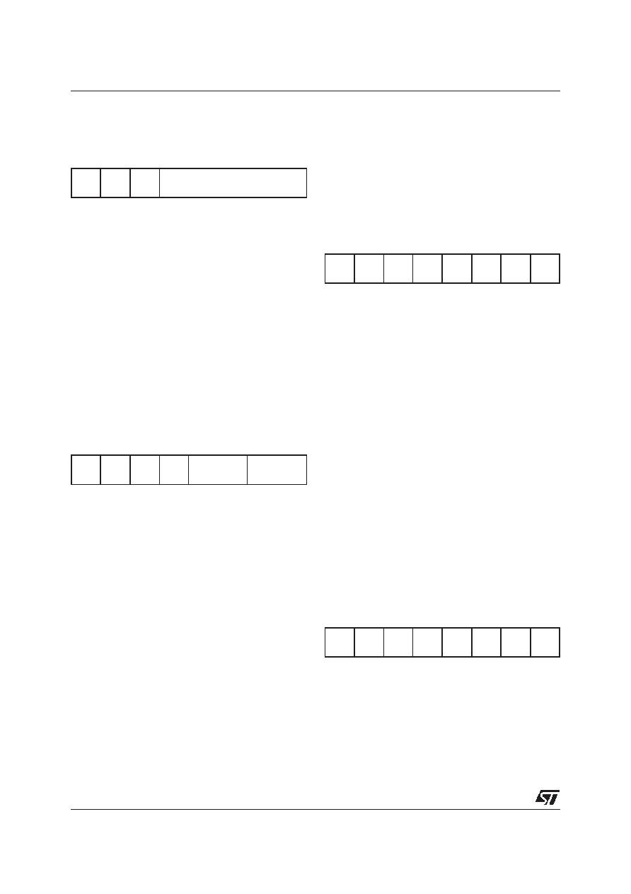
PWM/Timer 0 Control Register 2 (PWM0_CR2)
Configuration Register 10 (0Ah) Read/Write
Reset Value: 0000 0000 (00h)
Bit 7-6: Not Used
Bit 5: T0WAV T0OUT Waveform
0: pulse (type2)
1: square (type1)
Bit 4-0: T0PRESC PWM/Timer 0 Prescaler
The PWM/Timer 0 clock is divided by a
factor equal to 2T0PRESC. The maximum
value allowed for T0PRESC is 10000
(010h).
PWM/Timer 0 Control Register 3 (PWM0_CR3)
Configuration Register 11 (0Bh) Read/Write
Reset Value: 0000 0000 (00h)
Bit 7: T0SYNC PWM/Timer 0 Set/Reset mask
0: Set/Reset activated
1: Set/Reset masked
Bit 6: not used
Bit 5: T1SYNC PWM/Timer 1 Set/Reset mask
0: Set/Reset activated
1: Set/Reset masked
Bit 4: T0CKS PWM/Timer 0 Clock Source
0: Internal clock
1: External Clock from T0CLK
Bit 3-2: STRSRC PWM/Timer 0 Start signal source
00: Internal from T0STRT bit
01: External from T0STRT pin
10: Both internal and external
Bit 3-2: RESSRC PWM/Timer 0 Reset source
00: Internal from T0STRT bit
01: External from T0STRT pin
10: Both internal and external
Interrupt Polarity Register (INT_POL)
Configuration Register 1 (01h) Read/Write
Reset Value: 0000 0000 (00h)
Bit 7-6: Not Used
Bit 5: See LVD Registers Description
Bit 4: RESPOL Reset signal polarity
0: Reset on low level/falling edge
1: Reset on high level/rising edge
Bit 3: STRPOL Start signal polarity
0: Start on high level/rising edge
1: Start on low level/falling edge
Bit 2-0: See Interrupt Registers Description
12.5.2 PWM/Timer 0 Input Registers.
PWM/Timer 0 Counter High Input Register
(PWM0_COUNT_IN_H)
Input Register 21 (015h) Read only
Reset Value: 0000 0000 (00h)
Bit 7-0: T0CI15-8 PWM/Timer 0 Counter MSB
In this register the current value of the Timer 0
Counter MSB can be read.
74
0
-
T0WAV
T0PRESC
74
2
0
T0SYNC
-
T1SYNC T0CKS
STRSRC
RESSRC
70
-
LVD_EN RESPOL STRPOL POLPB
POLPA POLNMI
70
T0 CI15
T0CI14
T0CI13
T0CI12
T0CI11
T0CI1 0
T0 CI9
T0CI8
相關(guān)PDF資料 |
PDF描述 |
|---|---|
| ST52T430K3B6 | 8-BIT, OTPROM, 20 MHz, MICROCONTROLLER, PDIP32 |
| ST52T430K3T6 | 8-BIT, OTPROM, 20 MHz, MICROCONTROLLER, PQFP32 |
| ST5X86V12HS | 64-BIT, 120 MHz, MICROPROCESSOR, CPGA168 |
| ST6235Q6 | 8-BIT, MROM, 8 MHz, MICROCONTROLLER, PQFP52 |
| ST6240BQ6/XXX | 8-BIT, MROM, 8 MHz, MICROCONTROLLER, PQFP80 |
相關(guān)代理商/技術(shù)參數(shù) |
參數(shù)描述 |
|---|---|
| ST52F514Y3B6 | 制造商:未知廠家 制造商全稱:未知廠家 功能描述:Microcontroller |
| ST52F514Y3M6 | 制造商:未知廠家 制造商全稱:未知廠家 功能描述:Microcontroller |
| ST52F514YMM6 | 制造商:STMICROELECTRONICS 制造商全稱:STMicroelectronics 功能描述:8-BIT INTELLIGENT CONTROLLER UNIT ICU Two Timer/PWMs, ADC, I2C, SPI, SCI |
| ST-52K | 制造商:Eaton Heinemann 功能描述:ST52K |
| ST52N | 制造商:Eaton Corporation 功能描述: |
發(fā)布緊急采購,3分鐘左右您將得到回復(fù)。